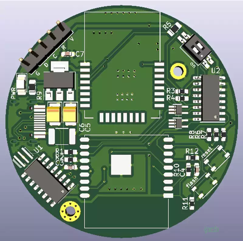
Round PCB Board is a printed circuit board whose shape is circular. It is commonly used in consumer electronics, wearable devices, etc.
Compared to traditional rectangular boards, round PCB board has the following significant advantages:
High space utilization: For devices that require tight integration and full use of internal space, such as miniature sensors, wearable devices, etc., a circular design can better fit the contours of the device shell, reduce wasteful corners, and improve space utilization.
Good structural strength: Circular structure has higher mechanical stability, which can resist external impacts and enhance the durability of the device.
Good EMC: Circular PCBs help reduce edge effects and optimize the EMC of circuits, especially for communication equipment with stringent requirements on signal quality.
Improved aesthetics: In certain products that focus on appearance design, such as high-end audio and smart watches, round PCBs can bring a more elegant and unified visual effect.
Round PCB Design
As we all know, designing circular PCBs is more tricky, and the tools on the market that support circular PCB design are quite limited. There are a number of specific design guidelines that must be followed when designing a circular PCB. For example, the edges of such boards can only be constructed by straight line segments. In addition, a circular outline needs to be depicted on the silkscreen layer when laying out the edge traces.
Design rules for circular circuit boards
First, CAD tools should be utilized to draw the basic shape of the circuit board.
If the circular circuit board is designed for high-speed equipment, it should usually be constructed as a multilayer printed circuit board.
The power and ground layers should be clearly delineated at different levels. A polygon editor can be used to define the specific shape of the ground or power layer.
Some software also provides special features to customize the power and ground layers.
When designing a circular circuit board, a suitable board-splicing scheme needs to be developed.
In order to panelize a circular PCB, a commonly used scheme is interrupted wiring. Spacing of at least 10 mm (approximately 0.39 inches) should be maintained between circular circuit boards.
In terms of mounting technology, surface mount technology (SMT) is more suitable for component placement than through-hole technology (THT).
Common circular PCB splicing methods.
- Ring splicing
Ring splicing is the most intuitive and efficient circular PCB splicing method, that is, a number of the same or different diameters of the circular PCB along the central axis of the sequential arrangement, the formation of a ring structure similar to the “nesting”. This splicing method is conducive to sharing the center power supply or data bus, simplify wiring, while facilitating heat dissipation. Applicable to the center processor as the core, the surrounding modules around the distribution of the system design. - Star splicing
Star splicing is a main control circular PCB in the center position, around the radial distribution of a number of sub-PCB, the main control PCB is responsible for system coordination and data exchange, sub-PCB to perform specific functions. This method is conducive to centralized control of signal transmission, reduce delay, suitable for distributed control systems or multi-channel data acquisition system. - Cellular splicing
Honeycomb splicing is similar to the honeycomb structure, where round PCBs of the same size are arranged in a hexagonal grid, and electrical interconnections are made between neighboring PCBs through connectors at the edges. This approach maximizes space utilization and provides good mechanical stability, and is commonly used in massively parallel processing systems or high-density sensor arrays.
With its unique shape and advantages, round pcb board is playing an increasingly important role in consumer electronics, wearable devices and other fields. Through efficient space utilization, excellent structural strength, good electromagnetic compatibility, and improved aesthetics, circular PCBs offer more possibilities for the design of modern electronic devices.