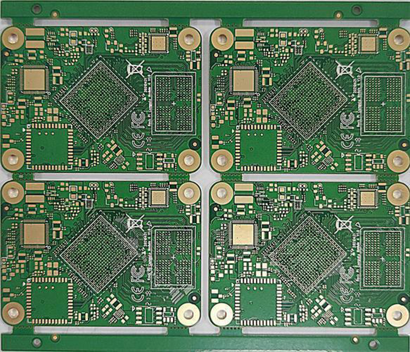
Anylayer HDI, as one of the most advanced processes in PCB manufacturing, enables interconnections between any layers within the board via laser blind vias, thereby achieving ultra-high routing density. The core of this process lies in the repeated execution of ‘Stacked Via’ and ‘Filled Via’ operations. Consequently, compared to conventional second-level HDI, its production complexity is significantly heightened, requiring greater attention to critical points throughout the manufacturing process.
Key Production Considerations for Anylayer HDI
- Material Selection
Importance:
Materials form the foundation; improper selection may cause subsequent processes to fail.
Considerations:
Substrate Material (PP Film)
Materials with excellent multi-lamination performance, well-matched resin content and flow properties, and high resistance to CAF (Cathodic Arc Failure) must be selected. Common examples include EM-825 and IT-968.
Core and Copper Foil
High Tg (glass transition temperature), low loss, and high Td (thermal distortion temperature) core materials are recommended, alongside high-performance reverse-tapered (RTF) or ultra-low profile (VLP/HVLP) copper foil to ensure fine line integrity and reliable bonding.
Via-Fill Copper Plating
Extremely high ductility and tensile strength are required to withstand rigorous thermal stress testing.
- Laser Drilling
Importance:
Laser-drilled vias form the core element of the Anylayer process, with their quality decisively impacting circuit interconnect reliability.
Precautions:
Precision Hole Form Control
Ensure perfectly straight and uniformly consistent hole walls, strictly avoiding ‘flared’ or conical hole shapes. Such defects cause plating irregularities and voids.
Alignment Accuracy Assurance
Each lamination cycle induces thermal expansion/contraction in the substrate. Therefore, compensation for this expansion/contraction must be applied prior to each laser drilling operation. This necessitates the use of high-precision laser drilling equipment with positioning accuracy within ±15μm, alongside Laser Direct Imaging (LDI) technology.
Media Material Adaptability Adjustment
Laser parameters—including energy, frequency, and pulse count—require meticulous fine-tuning based on the specific thickness and type of substrate material following each lamination process.
- Plating & Via Filling
Importance Statement:
Perfect via filling is the critical prerequisite for achieving stable stacked interconnections. Inadequate filling may lead to circuit board delamination or void formation during subsequent lamination processes.
Detailed Considerations:
Selection of Via Filling Plating Solution
It is imperative to employ a dedicated, high-performance via filling plating solution system. The balanced formulation of additives (encompassing accelerators, inhibitors, and levelling agents) is critically important, playing a decisive role in the quality of via filling.
Process Monitoring Essentials
Rigorously control the chemical composition of the plating solution through regular CVS analysis. Simultaneously, closely monitor solution temperature alongside the operational status of the agitation and filtration systems to ensure stable and reliable plating throughout.
Surface Dishing Control
Following via filling, surface dishing must be strictly controlled below 15μm. Excessive dishing causes uneven circuit surfaces or even circuit gaps, compromising electrical performance.
Copper Thickness Uniformity Assurance
Ensure consistent copper thickness across board surfaces and within vias to prevent ‘dog-boning’ effects caused by uneven current density distribution, which undermines circuit stability and reliability.
- Lamination and Registration
Importance:
Within the Anylayer process, multiple lamination steps constitute a common operational sequence. Each lamination cycle serves as a critical test of the preceding process outcomes, directly impacting the final product quality.
Key Considerations:
Contraction Control (Core Principle)
Data-driven Tracking Management
Number each substrate and laminate after every pressing operation, precisely measuring their expansion coefficients. Record this data to provide accurate compensation references for subsequent processes, ensuring pressing accuracy.
Standardised Process Execution
Adhere strictly to standard operating procedures during material pre-baking. Maintain stable pressing protocols, including appropriate heating rates, suitable pressure levels, and adequate vacuum conditions. These are critical factors in minimising random expansion phenomena.
Interface Cleanliness Maintenance
Prior to each lamination operation, ensure copper surfaces are clean and present suitable roughness. This is typically achieved through burnishing or plasma treatment to prevent delamination post-lamination.
Resin Loss Control Measures
Optimise the lamination process to ensure resin fully fills inter-track voids without excessive loss that could thin the dielectric layer, thereby compromising board performance.
- Circuit Imaging
Importance:
Anylayer processes typically require achieving ultra-fine line widths and spacings, generally demanding ≤2.5/2.5 mil. This imposes exceptionally high precision requirements on the circuit imaging process.
Considerations:
Adopting mSAP Process
Modified Semi-Additive Process (mSAP) is the ideal choice for producing ultra-fine circuits. This technique involves electroforming patterns onto thin copper substrates followed by rapid etching of the copper. Minimal side etching enables high precision, meeting Anylayer’s circuit fineness requirements.
LDI Application Requirements
Laser Direct Imaging (LDI) technology must be employed to eliminate expansion/contraction errors caused by temperature and humidity variations in traditional photomasks. This enables micron-level precision alignment, ensuring circuit fabrication accuracy and quality.
Frequently Asked Questions and Improvement Solutions
Issue 1: Interlayer Misalignment Beyond Tolerance
Symptoms:
In multilayer stacked structures, offset between bottom and top layer vias exceeds IPC-6013 standards, causing conductive path failure.
Root Causes:
- Inadequate compensation for cumulative panel deformation during multiple lamination cycles
- Drift in lamination equipment parameters or positioning system inaccuracies
- Slip induced by variations in interlayer dielectric thickness
Improvement Measures:
- Develop a dynamic expansion/contraction compensation model integrating AI algorithms to predict panel deformation trends
Upgrade lamination equipment to vacuum-assisted systems with closed-loop pressure control
Select MS-03A core board material with low CTE (≤14ppm/℃)
Issue 2: Via Filling Defects (Voids/Surface Depressions)
Symptoms:
Post-electroless plating:
Copper coverage within vias <95% (IPC-TM-650 inspection) Vias mouth indentation depth >12μm (compromising subsequent pattern transfer accuracy)
Root Causes:
Abnormal concentration of leveling agent in plating solution
Inappropriate pulse plating waveform parameter settings
Laser drilling taper angle >120° causing bubble entrapment
Improvement Measures:
Implement online CVS (Cyclic Voltammetric Stripping) for real-time additive concentration monitoring
Adopt reverse pulse plating technology with a pulse ratio of 3:1
Optimise laser drilling parameters: implement gradient-decreasing pulse energy control
Issue 3: Interlayer Separation (Blistering)
Symptoms:
Post-288°C immersion tin test:
Interlayer peel strength < 1.0 N/mm (IPC-6013 Class 3 requirement ≥ 1.5 N/mm)
Bubble-like protrusions at blind hole bottoms
Root causes:
Copper surface roughness (Rz) > 5 μm post-brown treatment
Pressing temperature rise rate > 3°C/min causing resin curing stress concentration
Via-filling material glass transition temperature (Tg) < 170°C
Improvement Measures:
Employ nano-scale brownisation process, controlling Rz within 2.5-3.5μm range
Implement stepped pressing curve: heating phase ≤ 2°C/min, holding phase ±1°C
Select high-Tg (≥210℃) LCP substrates to replace conventional FR-4
Issue 4: Surface Copper Thickness Variation
Symptoms:
Panel copper thickness variation >15% (IPC-4562 standard requires ≤10%), resulting in:
Incomplete etching of fine traces (≤15μm)
Impedance control deviation >±8%
Root Cause:
Electroplating line cathode movement speed fluctuation >5%
Insufficient density of auxiliary anodes (Thief Pads)
Uncompensated current shielding effect at board edges
Improvement Plan:
Upgrade electroplating line to variable frequency drive system, controlling speed fluctuation within ±2%
Employ AI-assisted layout algorithms during CAM design phase to optimise Thief Pad distribution
Add conductive edge frame design at board perimeter, width ≥15mm
Issue 5: Laser Drilling Anomalies
Symptoms:
Hole wall inspection reveals:
Resin carbonisation layer thickness > 3μm (SEM observation)
Glass fibre debris residue at hole bottom
Root Causes:
Laser wavelength (1064nm) mismatched with material absorption coefficient
Focused spot diameter > 25μm (design requirement ≤ 20μm)
Auxiliary gas pressure fluctuation > 0.5 bar
Improvement Measures:
Switch to 532nm green laser to enhance material absorption
Implement automatic focus compensation system for real-time depth-of-focus deviation correction
Employ nitrogen-helium mixed gas (3:1 ratio) to stabilise gas flow
As a cutting-edge technology in PCB manufacturing, the Anylayer HDI process encompasses multiple critical stages including material selection, laser drilling, electroplating via filling, lamination alignment, and circuit formation. Each stage plays a decisive role in determining the final product’s performance and quality. In practical production, common challenges such as interlayer alignment deviations, via filling defects, delamination, surface copper thickness irregularities, and laser drilling quality issues present significant production hurdles.
However, by thoroughly analysing the root causes of these issues and implementing targeted improvement measures—such as developing dynamic compensation models, optimising plating parameters, and upgrading materials and equipment—these challenges can be effectively overcome. This enhances the production standards and product quality of Anylayer HDI processes, propelling the PCB manufacturing industry towards higher precision and greater reliability.
