Understanding Semiconductor Substrates
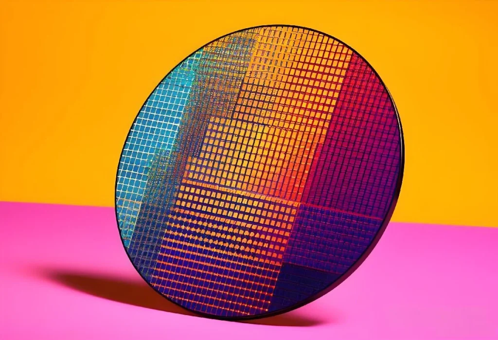
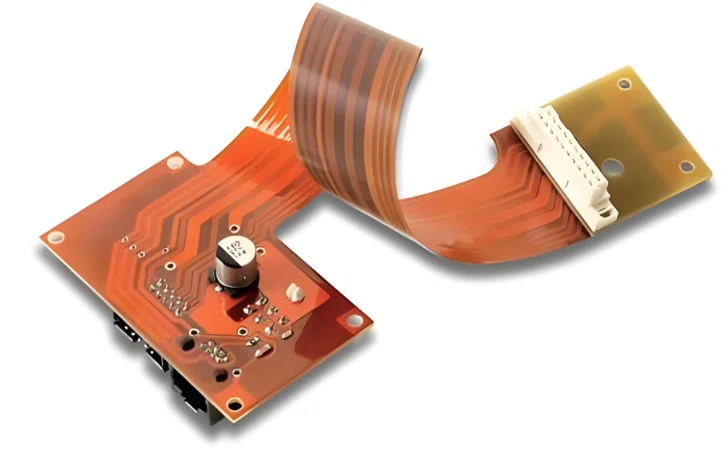
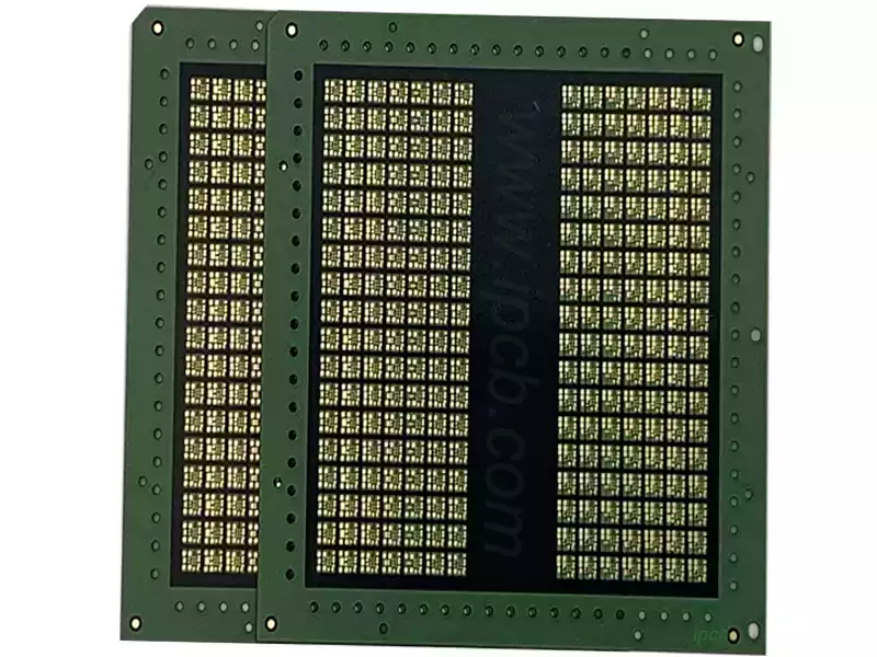
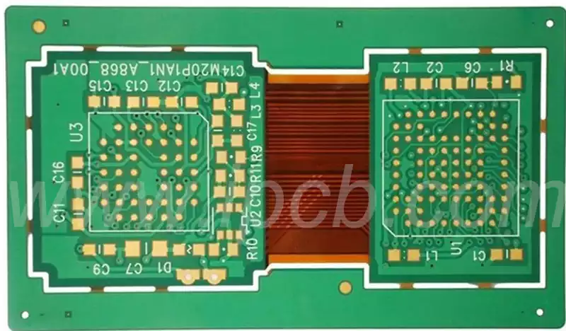
In the semiconductor industry, semiconductor substrates play a crucial and fundamental role. Whether it’s microprocessors, memory, power devices, or RF modules, substrates are the physical support platform upon which these electronic devices rely.
They not only support the physical structure of the device but also directly influence its electrical performance, heat dissipation, and mechanical stability. Throughout the semiconductor industry chain, substrates serve as a bridge connecting materials science, process technology, and end applications, determining the feasibility and efficiency of upstream material selection and downstream device manufacturing.

The role of semiconductor substrates goes beyond simply supporting the chip itself. Their properties, such as electron mobility, thermal conductivity, and mechanical strength, directly impact the chip’s operating speed, power consumption, and reliability. For example, in high-performance processors, the substrate’s thermal conductivity determines the chip’s temperature rise under prolonged, high-load operation, thus impacting system stability. In power devices, the substrate’s electrical insulation and thermal management capabilities determine the device’s safe operating voltage and lifespan. Therefore, substrates are not only physical supports but also a core component in optimizing semiconductor performance.
Furthermore, as semiconductor applications continue to expand, the importance of substrates becomes increasingly prominent. 5G communications, artificial intelligence computing, efficient power conversion, and new energy applications all place higher demands on devices, and these demands often manifest themselves first in challenges to substrate materials and processes.
For example, high-speed signal transmission requires materials with low dielectric loss, high-power devices require substrates with high thermal conductivity and high breakdown voltage, and high-reliability applications demand substrates with extremely low defect density and a uniform crystal structure. Therefore, semiconductor substrates are an irreplaceable strategic resource, both from the perspectives of industry chain management and technological research and development.
Semiconductor Substrate Types and Characteristics
The type and material properties of a semiconductor substrate directly determine its applicability and performance in electronic devices. Traditional semiconductor substrates are primarily made of silicon (Si), due to its excellent semiconductor properties, mature processing technology, and well-established supply chain. Single-crystal silicon substrates are widely used in the manufacture of microprocessors, memory devices, and power devices, offering a uniform crystal structure, stable electrical performance, and high mechanical strength.
The electron mobility of silicon substrates is moderate, but sufficient to meet the high-speed computing requirements of most conventional logic circuits. Furthermore, their high-temperature stability and thermal conductivity enable chips to operate normally in low- and medium-power applications. For manufacturers, silicon substrates are easy to cut, grind, and polish, resulting in higher chip yields and relatively manageable costs. This is a key reason why silicon has long dominated the semiconductor market.
However, as semiconductor devices evolve toward high-frequency, high-power, and high-temperature environments, relying solely on silicon substrates is no longer sufficient to meet the demands of specific applications. In high-speed communications or RF devices, materials with high electron mobility and low dielectric loss can significantly improve signal transmission speed and system efficiency. In power devices, substrates must withstand high voltages and high temperatures while also possessing excellent thermal conductivity to ensure stable and reliable device operation. Therefore, in addition to traditional silicon substrates, advanced materials such as gallium arsenide (GaAs), silicon carbide (SiC), and gallium nitride (GaN) are gradually entering the market and demonstrating unique advantages in specific applications.
GaAs substrates, with their high electron mobility and wide bandgap, excel in RF and high-speed communications. Their material properties enable GaAs devices to maintain low noise and high efficiency at high frequencies, making them ideal for microwave amplifiers, satellite communications, and optical communication modules. However, GaAs substrates are expensive to produce, and the crystal growth and cutting processes are complex, requiring strict control of crystal defects and doping uniformity.
Silicon carbide and gallium nitride substrates are primarily used in high-power, high-temperature, and high-efficiency applications. SiC, with its high thermal conductivity, high breakdown voltage, and wide bandgap, is gradually replacing traditional silicon devices in electric vehicle inverters, power converters, and industrial power modules. GaN substrates offer advantages in high-frequency, high-power applications, including smaller size, lower energy consumption, and higher efficiency, making them particularly suitable for RF power amplifiers and 5G communication base stations.
The performance of semiconductor substrates depends not only on the material itself but also on multiple factors, including thickness, doping concentration, crystal defectivity, and surface roughness. For example, crystal defects can reduce electron mobility and shorten carrier lifetime, thereby affecting device switching speed and power consumption. Excessive surface roughness can lead to poor packaging, soldering defects, and even chip damage.
Precision processing and rigorous testing of substrates are essential for high-performance chip manufacturing. Through techniques such as grinding, polishing, and epitaxial processing, nanometer-level surface flatness can be achieved, providing precise support for micron- and even nanometer-scale device structures.
Furthermore, differences in mechanical strength, thermal expansion coefficient, and chemical stability among different substrate types directly impact chip packaging, heat dissipation, and reliability design. For example, high-power devices generate significant heat during operation. If the thermal expansion coefficient of the substrate does not match that of the packaging material, this can lead to stress concentration in the device, causing package failure or solder joint fracture. Low thermal conductivity materials can cause heat accumulation, significantly shortening device life. Therefore, the selection of substrate materials must be comprehensively evaluated based on the chip application scenario, operating conditions, and process requirements.
New Alternatives to Silicon: The Rise of Advanced Materials Such as GaAs, SiC, and GaN
As semiconductor technology continues to advance toward higher frequencies, higher powers, and higher reliability, traditional silicon substrates are increasingly showing their limitations in certain applications, driving the rise of advanced semiconductor substrates such as gallium arsenide (GaAs), silicon carbide (SiC), and gallium nitride (GaN). These substrate materials offer significant advantages over silicon in terms of electron mobility, bandgap width, thermal conductivity, and breakdown voltage, making them irreplaceable key materials in RF communications, power electronics, laser devices, and optoelectronics.
The development of advanced substrates not only meets performance requirements but also drives the technological advancement of device miniaturization, higher power, and system integration, gradually forming a new strategic landscape within the semiconductor industry.
Gallium arsenide substrates, due to their high electron mobility and wide bandgap characteristics, have long dominated the field of high-frequency RF and optoelectronic devices. In microwave amplifiers, satellite communication modules, and optical communication systems, GaAs devices provide excellent signal gain and low noise performance, which are crucial for modern high-speed communication systems. Compared to silicon substrates, GaAs substrates exhibit lower dielectric loss and faster response speed at high frequencies, but their production process demands extremely high standards, including defect control during crystal growth, doping uniformity, and precise surface treatment. Despite its higher cost than silicon substrates, GaAs maintains strong demand in high-end RF and optoelectronic applications due to its irreplaceable performance.
Silicon carbide substrates have rapidly gained popularity in high-power applications in recent years, particularly in electric vehicles, power inverters, and industrial energy management. SiC substrates offer high thermal conductivity and breakdown voltage, allowing them to withstand extremely high temperatures and current densities. This makes SiC devices far superior to traditional silicon devices in terms of high-efficiency power conversion and durability. Their wide bandgap also allows them to operate stably at higher voltages and temperatures, reducing system cooling requirements and improving overall efficiency. However, SiC substrates are challenging to manufacture, with complex crystal growth and epitaxial deposition techniques and high processing costs, limiting their application to the high-end power electronics market.
GaN substrates, with their high electron mobility and wide bandgap, demonstrate exceptional efficiency in high-frequency, high-power applications. GaN substrates enable smaller devices and lower energy consumption, attracting significant interest in 5G communication base stations, high-frequency radar, and power electronics. Similar to SiC, the production process for GaN substrates is complex, requiring precise control of epitaxial deposition, defect control, and thermal management to ensure device performance and reliability. As GaN technology matures, its application prospects in RF power devices and power conversion systems continue to expand, driving the development of the related global industry chain.
Beyond the inherent advantages of the material itself, the development of these advanced semiconductor substrates is closely tied to specific application scenarios. High-frequency communications require low dielectric loss and high signal rates, while high-power power supplies and electric vehicles demand high thermal conductivity and breakdown voltage. High-reliability electronic systems demand low crystal defectivity and high mechanical stability. Substrates of different materials have emerged precisely to meet these diverse needs, each forming its own technological barriers and industry advantages. Crystal growth, epitaxial deposition, and polishing and cutting technologies at the upstream end of the industry chain are closely linked to downstream packaging, heat dissipation, and system integration, collectively determining the performance and reliability of high-end semiconductor devices.
The Precision of Manufacturing Processes—From Crystal Growth to Polishing and Packaging
The value of semiconductor substrates lies not only in the material itself but also in the sophisticated and complex manufacturing process. A high-performance substrate requires not only ideal material properties but also precise control of every step from crystal growth to final packaging, which determines the chip’s yield, performance, and reliability. The precision and consistency of the manufacturing process are key factors in semiconductor devices’ ability to meet high-frequency, high-power, and high-reliability requirements, and are also the core criteria that distinguish standard substrates from high-end ones.
Crystal growth is the first and most critical step in semiconductor substrate manufacturing. For silicon, for example, the commonly used Czochralski (CZ) and Float Zone (FZ) methods can produce high-purity, single-crystal silicon ingots, laying the foundation for subsequent cutting and processing. During the crystal growth process, parameters such as doping concentration, temperature gradient, and crystal pulling speed require precise control to ensure a uniform crystal structure, low defect density, and the required electrical and mechanical properties.
Any slight deviation can lead to lattice defects, stress concentration, or reduced electron mobility, thus affecting the final device performance. In high-end applications such as RF, power devices, and high-speed logic chips, the requirements for crystal integrity and defectivity are even more stringent, necessitating strict quality management and high-precision equipment support during the crystal growth process.
After crystal growth, the substrate typically undergoes precision processing steps such as cutting, grinding, and polishing to achieve nanometer-level surface flatness and thickness uniformity. This process not only affects the replication accuracy of the chip’s micron-scale structures but also determines the package’s fit and thermal conductivity.
For example, in power device packaging, excessive surface roughness increases thermal resistance, reducing device heat dissipation efficiency. In RF device packaging, surface unevenness can lead to unstable interconnects or increased signal loss. The grinding and polishing processes require extremely high equipment precision and meticulous management of material properties, stress distribution, and processing temperature to ensure that the physical properties of each substrate precisely meet design requirements.
Epitaxial growth and thin-film deposition are also essential steps in the manufacturing process, especially for advanced material substrates such as GaAs, SiC, and GaN. Chemical vapor deposition (CVD), molecular beam epitaxy (MBE), or metal-organic chemical vapor deposition (MOCVD) techniques can be used to grow high-quality epitaxial layers on the substrate surface, providing an ideal electron migration environment and electrical performance for the device.
The uniformity, thickness control, and defect density of the epitaxial layer directly impact the chip’s switching speed, power consumption, and thermal stability. For high-power, high-frequency applications, the precision requirements of the epitaxial process are even higher than those of the substrate itself, as the performance of the epitaxial layer determines the reliability of the device under extreme conditions.
Finally, the substrate undergoes processes such as packaging adaptation, thermal management design, and quality testing to ensure its stability during chip assembly and system application. The packaging process must consider the substrate’s thermal expansion coefficient, thermal conductivity, and mechanical strength to prevent cracks, warping, or solder joint fracture during high-temperature, high-power operation.
Meanwhile, precision testing technologies such as X-ray crystal defect analysis, surface roughness measurement, and doping concentration testing ensure that each substrate meets stringent performance specifications. In high-end chip mass production, these processes are closely linked, and deviations in any one step can lead to device performance degradation or reduced yield, highlighting the precision and complexity of semiconductor substrate manufacturing.
Semiconductor substrate manufacturing is not just a material processing process; it also presents a comprehensive challenge to physics, chemistry, and process technology. Every process requires high-precision control and strict quality management, from crystal growth, cutting, grinding, and polishing to epitaxial deposition and packaging testing. This not only ensures device performance and reliability but also provides a solid foundation for high-frequency, high-power, and high-end applications. Furthermore, this process precision reflects the semiconductor industry’s high demand for technological innovation and process optimization, and is a key indicator of industry competitiveness.
In short, the semiconductor substrate manufacturing process is complex and precise, with every step directly impacting device performance and reliability. From crystal growth uniformity to nanometer-level flatness during polishing, to epitaxial layer deposition and packaging inspection, each step requires high precision and strict control. Only under strict manufacturing process control can semiconductor substrates maximize their value and provide reliable support for chip performance improvement and industrial development.
The Relationship between Semiconductor Substrates and Chip Performance
The semiconductor substrate is not only the physical carrier for device manufacturing but also one of the fundamental factors determining chip performance. It directly affects electrical characteristics, thermal management capabilities, signal integrity, and device reliability. It can be said that the upper limit of chip performance is often determined by the quality and design of the substrate. With the continuous reduction of process nodes and the continuous increase in packaging integration, the requirements for substrate performance are becoming increasingly stringent.
First, electrical performance is the most intuitive indicator. Substrate parameters such as dielectric constant, dielectric loss, and conductivity directly impact signal transmission speed and energy loss. For high-speed communication chips, for example, signal frequencies often exceed tens of GHz. If the substrate’s dielectric loss is high, the signal will be significantly attenuated during transmission, resulting in eye closure and increased bit error rates. Using substrate materials with a low dielectric constant (Dk) and low dissipation factor (Df) can significantly improve signal integrity and system speed. Furthermore, doping concentration and uniformity are crucial to the chip’s electrical conductivity. Tiny impurities in the crystal can create localized electric fields, reducing carrier mobility and thus limiting device switching speed.
Therefore, a substrate with excellent electrical properties is a prerequisite for implementing high-speed logic circuits, radio frequency communications, and high-frequency amplifiers.
Secondly, thermal performance determines a chip’s power density and reliability. As modern chips continue to increase in integration density, power consumption increases accordingly. Ineffective heat dissipation leads to elevated junction temperatures, impacting device lifespan and operational stability. Substrates with high thermal conductivity, such as aluminum nitride (AlN), silicon carbide (SiC), and diamond, efficiently dissipate device heat and prevent localized overheating.
In particular, thermal management has become a critical performance metric in power electronics, automotive electronics, and radar modules. In comparison, traditional silicon substrates have lower thermal conductivity and require optimization with metal heat dissipation layers or thermal interface materials (TIMs). For this reason, the use of high-thermal-conductivity substrates in high-power applications has rapidly increased in recent years, driving device miniaturization and higher power density.
Third, mechanical properties and structural stability are also key factors influencing chip reliability. Chips experience temperature cycling, mechanical stress, and packaging strain during long-term operation. If the coefficient of thermal expansion (CTE) of the substrate does not match that of the chip material, warping, cracking, and even solder joint failure can occur. For example, wide-bandgap materials such as SiC and GaN offer excellent performance at high temperatures, but their CTE differs significantly from that of the packaging material. Therefore, thermal stress mitigation requires substrate design, optimized packaging structure, or the addition of interlayers. These engineering details directly impact chip stability and lifespan.
Furthermore, surface flatness and defect density also have a significant impact on chip performance. Nanoscale device structures require an extremely smooth substrate surface; otherwise, lithographic patterns are easily distorted, impacting device linewidth uniformity and parasitic control. Crystal defects such as microcracks, dislocations, and voids can propagate during subsequent processing, causing leakage, breakdown, or device failure. High-quality substrates undergo rigorous polishing and inspection processes to ensure surface roughness below 1 nm and defect density below 10⁴ cm⁻², thereby improving device yield and long-term reliability.
Furthermore, electromagnetic compatibility and signal integrity are becoming increasingly important in high-speed packaging design. With the development of 5G, AI chips, and high-speed storage, signal frequencies have increased significantly, making electromagnetic coupling effects more prominent. High-performance substrates utilize multi-layer wiring structures, shielding designs, and optimized dielectric layers to reduce crosstalk and reflections, ensuring signal phase alignment and stable data transmission. In particular, in multi-chip modules (MCMs) and system-in-package (SiPs), substrates not only provide mechanical support but also serve as a core platform for signal distribution and power management.
Finally, from a system perspective, improved substrate performance often leads to overall system optimization. Higher thermal conductivity reduces the size of heat dissipation components; lower dielectric loss reduces power consumption and improves energy efficiency; and improved mechanical strength extends service life. In other words, semiconductor substrates not only influence the performance of individual chips but also determine the efficiency and stability of the entire electronic system. As chip design evolves towards higher frequencies, higher powers, and greater integration, the role of the substrate has shifted from a “carrier” to a “performance amplifier,” becoming an indispensable core element in system engineering.
In summary, the semiconductor substrate is inextricably linked to chip performance. It determines signal propagation speed and energy loss, while also impacting thermal management, structural reliability, and system stability. Whether from the perspective of material selection or process optimization, improving substrate performance is a key path to achieving high-performance chips. In the future, with the continuous advancement of new materials and packaging technologies, semiconductor substrates will continue to play a core role in achieving performance breakthroughs and revolutionizing energy efficiency.
Key Processes and Quality Control in Semiconductor Substrate Manufacturing
The manufacturing process of semiconductor substrates is one of the links with the highest technical barriers in the entire industry chain. Although the substrate may appear to be a single piece of material, every step, from raw material purification to crystal growth, slicing, grinding, polishing, and final testing, determines its crystal integrity, electrical performance, and reliability. Even the slightest fluctuation in substrate quality can have a ripple effect on subsequent chip manufacturing, packaging, and even the performance of the final product. Therefore, understanding the manufacturing process and quality control logic is key to understanding the essence of the semiconductor industry.
First, material purity and crystal growth technology are the core of the manufacturing process. Taking silicon substrates as an example, the first step in their production is the extraction of high-purity polysilicon. Purity typically needs to reach “11 nines” (99.999999999%) or higher; otherwise, impurity ions will severely affect carrier mobility and breakdown voltage. Single crystal silicon rods are then grown using the Czochralski (CZ) or melt-zone (FZ) methods. The crystal orientation (e.g., <100> or <111>) must be precisely controlled based on the target device type and performance requirements.
For compound semiconductors such as GaAs or SiC, crystal growth is more challenging, and methods such as liquid phase epitaxy (LPE), molecular beam epitaxy (MBE), or chemical vapor deposition (CVD) are often used to achieve low defect density and good compositional uniformity. If stress, dislocations, and microcracks within the crystal are not controlled at this stage, they will be amplified in subsequent steps, leading to increased wafer scrap rates.
Secondly, wafer dicing and surface processing determine the geometric accuracy and mechanical strength of the substrate. After orientation and slicing, the crystal rods are cut using precision wire saws or lasers to control thickness and edge shape. Saw marks and microcracks often remain on the surface of the sliced wafers, necessitating multiple grinding and polishing steps to achieve nanometer-level flatness. CMP (chemical mechanical polishing) technology is crucial in this process. It combines chemical etching with mechanical grinding to remove surface damage and optimize surface finish. High-end semiconductor substrates require a surface roughness (Ra) of less than 1nm, which not only affects the accuracy of subsequent photolithography but also determines the quality of epitaxial layer growth.
Next comes epitaxial growth and doping control. Growing an epitaxial layer (epi layer) on a silicon or compound substrate allows for structures with specific resistivity and carrier concentration to meet the requirements of different chips. For example, power devices require precise doping to achieve high breakdown voltage and low on-resistance, while RF chips demand extremely low defect density and high mobility. During the epitaxial growth process, gas flow, temperature gradient, and reaction rate all require strict control; even the slightest deviation can lead to uneven layer thickness or impurity contamination. Today, MOCVD (metal-organic chemical vapor deposition) equipment achieves atomic-level precision, ensuring the mass production of wide-bandgap materials such as GaN and SiC.
After epitaxial growth, surface cleaning and defect detection become key quality control steps. Semiconductor manufacturing requires extremely high cleanliness levels, and even trace amounts of organic residue, metal ion, or particle contamination can cause device failure. Common cleaning methods include RCA cleaning, ultrasonic deionized water cleaning, and plasma decontamination. After cleaning, surface flatness, lattice distortion, and defect density are inspected using optical microscopes, interferometers, X-ray diffraction (XRD), atomic force microscopes (AFM), and other instruments. The allowable defect density for top-tier substrates can be as low as 10² cm⁻², orders of magnitude lower than that of common electronic materials.
Thickness uniformity and warp control are also important indicators of substrate quality. Because wafers are prone to stress deformation at high temperatures, manufacturers typically incorporate stress-balancing mechanisms during the polishing and heat treatment stages. Some high-end production lines also employ laser interferometry systems to monitor warp in real time and automatically correct for it, achieving submicron accuracy. This high-precision control not only improves yield but also ensures device alignment accuracy and mechanical stability during the packaging process.
Finally, quality inspection and factory verification conclude the entire process and form the foundation of supply chain trust. Before leaving the factory, every substrate undergoes rigorous resistivity testing, TTV (total thickness variation) inspection, surface defect scanning, and thermal conductivity verification. Some high-end customers also require full-process SPC (Statistical Process Control) reports to track production stability. Substrates used in power electronics or automotive applications also undergo high-temperature aging, thermal cycling, and mechanical shock testing to ensure stable performance even under extreme conditions.
In summary, semiconductor substrate manufacturing is a systematic process that integrates materials science, precision machining, and quality control. From raw material purity to crystal integrity, from surface polishing to epitaxial growth, every step has a decisive impact on final performance. It is these seemingly “invisible” manufacturing details that lay the technological foundation for the entire semiconductor industry. In the future, with the introduction of new materials and intelligent manufacturing technologies, the precision and consistency of substrate manufacturing will be further improved, helping semiconductor devices reach a new level of higher performance and reliability.
Summary
Semiconductor substrates are not only the foundational material for chip manufacturing but also a core factor that determines device performance, reliability, and system efficiency. From traditional silicon substrates to advanced materials such as GaAs, SiC, and GaN, substrate development is closely linked to materials science, manufacturing processes, and quality control. Crystal growth, cutting and grinding, epitaxial deposition, surface polishing, and rigorous testing—each step directly impacts the chip’s electrical performance, thermal management capabilities, mechanical stability, and signal integrity. High-performance substrates play a critical role in applications such as high-speed communications, power electronics, RF devices, artificial intelligence, and electric vehicles. Their technical precision and reliability determine the innovation and development of the entire semiconductor industry.


