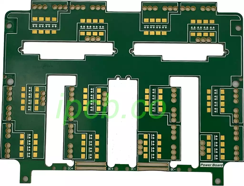
PCB solder mask, also called solder resist, is a polymer coating applied over the copper conductors of a printed circuit board. It does two jobs. It protects the copper from environmental corrosion, especially oxidation, and it stops solder from bridging between pads. During reflow or wave soldering, where molten solder is hard to control precisely, the mask keeps solder on the pads it is meant for.
“Solder resist” is the more accurate name, because “solder mask” can be confused with the solder layer itself. Both terms mean the same coating.
This page covers the mask types, the six-step process with typical parameters, the surface finish that follows, and thickness. For detail on specific topics, follow the links to our thickness guide and our minimum solder mask sliver guide.
Types of PCB Solder Mask
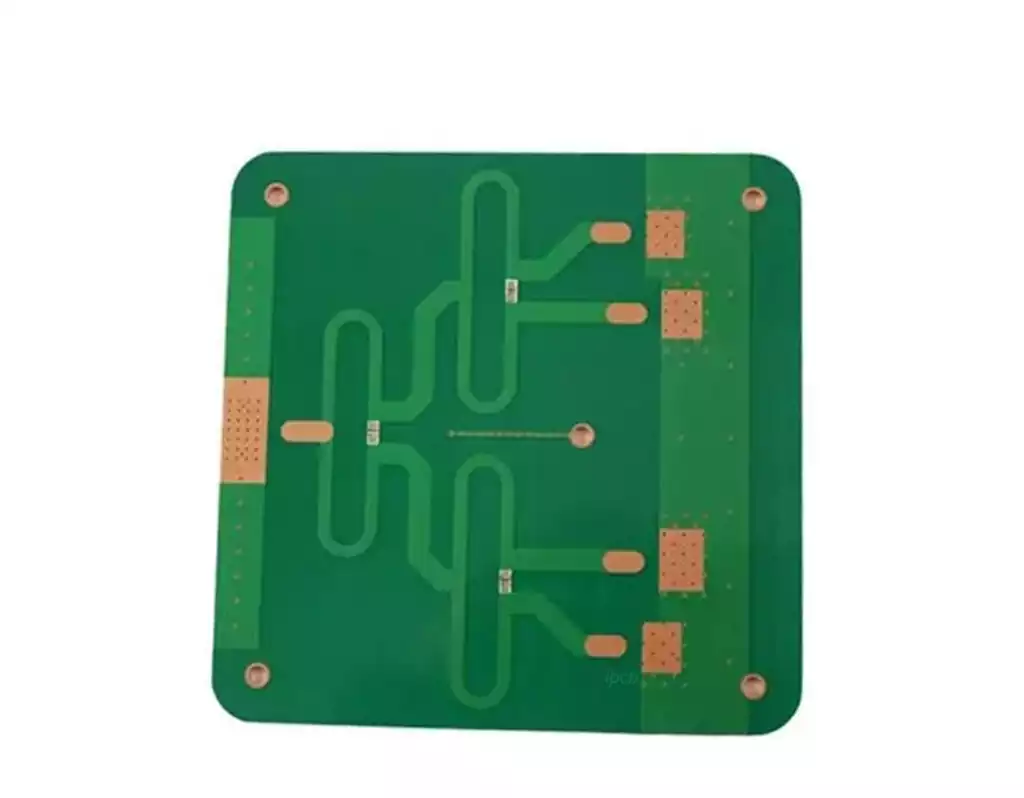
Which type to use is a trade-off between cost and what the pcb board needs. The simplest approach is to screen-print liquid epoxy over the conductors. Photoimageable types give finer openings. Solder Mask comes in several colors. Green is the most common, and red, blue, black, white and yellow are also available.
Liquid Epoxy Solder Mask
Liquid epoxy is the most basic and economical option. The resin is screen-printed onto the board: a woven mesh supports a stencil pattern, and ink passes through only the open areas. Epoxy is a thermosetting polymer, so it hardens gradually during thermal curing. Dyes are added to the resin to get the required color.
Liquid Photoimageable (LPI) Solder Mask
LPI mask, which the previous version of this page called LPSM, uses photolithography, much like photoresist exposure in semiconductor manufacturing. It can be applied by screen printing or by spraying, and spraying is usually the cheaper of the two. Photolithography defines the openings around pads, vias and mounting holes far more precisely than printing alone.
In practice the sequence is:
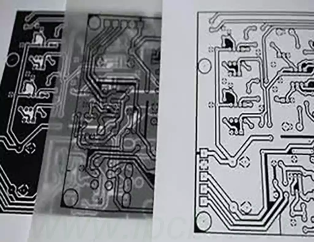
Photomasks matching the mask pattern are made from the Gerber files. See Gerber files in PCB manufacturing.
The panel is cleaned so no dust or contamination ends up under the cured mask.
LPI is coated over both sides and dried.
The board is exposed to UV through the photomask. Clear areas let the UV through and cure the mask that stays. Dark areas block the UV, so the mask there stays soft and is washed away, which forms the openings over pads.
Dry Film Solder Mask (DFSM)
The dry film flow is similar to LPI and also uses photolithographic exposure. The difference is that the mask is a film, laminated onto the board under vacuum. Vacuum lamination makes the film adhere tightly and removes air bubbles. After exposure, solvent removes the unexposed areas and the remaining film is thermally cured. See dry film solder mask in PCB manufacturing.
Top and Bottom Layer Masks
Some guides list “top” and “bottom” masks as types. These words only say which side of the board the mask is on. They are not a process or a material.
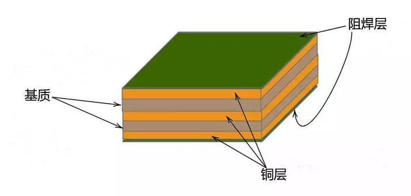
Solder Mask Process Flow
The process is often reduced to “apply green ink, then dry”. In fact it has six steps, and each affects properties such as adhesion and resolution.
| Step | What it does | Typical parameters* |
|---|---|---|
| Pre-treatment | Removes grease, oxide and contamination so the mask grips both laminate and copper. Includes degreasing (ultrasonic, alkaline, checked with a water-film test), micro-etching and hot-air drying. | Micro-etch with ammonium persulfate, roughening depth about 1–1.5 µm |
| Coating | Covers the board evenly by screen printing or spraying, in a dust-controlled room. | Film about 10–30 µm, adjusted to the requirement |
| Pre-baking | Drives off solvent such as xylene so the mask goes from liquid to semi-solid and does not stick to the artwork during exposure. | About 70–80 °C for 20–30 min; finish should be tack-free with under 1% residual solvent |
| Exposure | UV cures the areas that must remain. This is the step that forms the pattern. | Alignment deviation under about 0.05 mm; about 80–120 mJ/cm² for 10–20 s for liquid photoimageable mask |
| Development | Developer dissolves the unexposed mask and opens the pads. Afterwards, openings should be free of residue and the remaining mask intact. | About 1–2% sodium carbonate at 30–35 °C for 60–90 s, then a 3–5 min deionized-water rinse |
| Curing | Final hardening. Liquid epoxy is cured by heat. LPI and dry film are first cured by UV during exposure, then thermally cured. | About 150–160 °C for 60–90 min, with staged heating to avoid cracking |
Typical values carried over from the previous version of this page. Real values depend on the ink supplier’s data sheet and on the line, so treat them as a guide and not as a spec.
Surface Finish After Solder Mask
Whatever mask type is used, some copper stays exposed. Those areas need a surface finish to prevent oxidation and keep them solderable. The most common finish is hot air solder leveling, see HASL finish analysis. ENIG (electroless nickel immersion gold) and ENEPIG (electroless nickel, electroless palladium, immersion gold) are also widely used, see ENIG plating. Where solder paste is applied, apertures are reserved for it and processed according to the manufacturing requirements.
PCB Boards with gold fingers can combine finishes. One approach is to plate electroless nickel-gold on both the fingers and the pads, apply a blue peelable mask, and then electroplate thick hard gold on the fingers only.
Standard Solder Mask Thickness
Solder Mask thickness depends mainly on the thickness of the copper traces beneath it. In open areas, LPI and dry film thickness varies by location. The figures given here come from the previous version of this page:
Starting film thickness: typically about 0.5 mil.
Open areas: an average of about 10–18 µm.
Over traces: about 0.5 mil of coverage is generally needed.
At conductor edges: the mask thins and can reach 0.3 mil or less.
IPC minimums: the page cited 10 µm for Class 2 and 18 µm for Class 3.
Sprayed epoxy mask gives a more uniform thickness across the board. For how to choose a value, read PCB solder mask thickness: selection and application.
Solder Mask Relief and Why It Matters
The mask does more than protect copper. It also forms a barrier between adjacent pads. Around each component pad, a small gap called solder mask relief is left between the mask edge and the pad. This keeps solder from bridging, which is critical for high-density parts such as fine-pitch BGAs, and it leaves the pad free so solder can wet it fully and hold the component in place. For design guidance, see solder mask openings, minimum solder mask sliver and BGA PCB design.
The right solder mask type and a well-controlled process together decide whether a board is reliable and repeatable. Liquid epoxy is cheap and simple, LPI gives fine openings at reasonable cost, and dry film suits dense boards that need uniform thickness. Confirm type, color, thickness and finish with your fabricator before release.