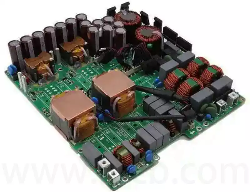
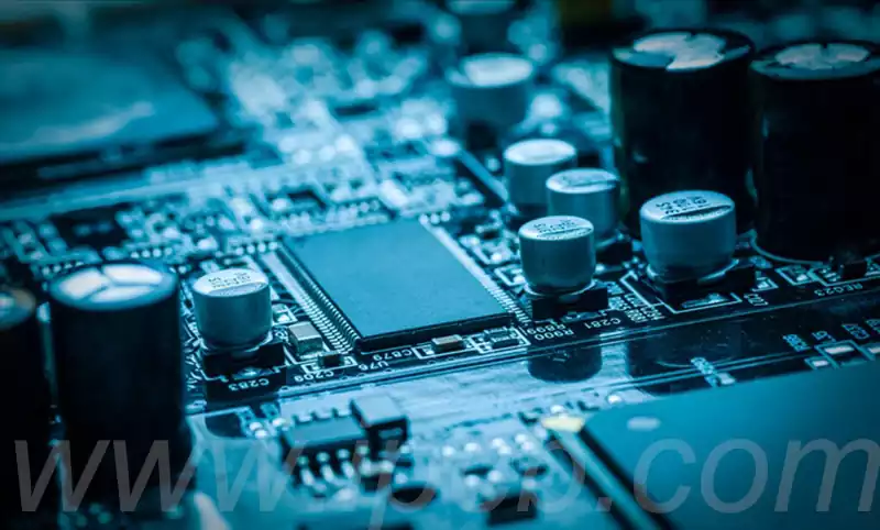
Laser engraving pcb board is a process that employs laser technology to etch and process printed circuit boards. This technique is commonly used for PCB marking, cutting, copper layer removal, or other specific machining requirements. Compared to traditional chemical etching or mechanical machining methods, laser engraving offers advantages such as high precision, rapid processing, non-contact operation, and a minimal heat-affected zone. It finds extensive application in the production of high-precision circuit boards, prototyping, specialised identification, and processing certain specific materials.
The technical principle of laser engraving PCB board primarily relies on the high energy density of the laser beam, precise control, and its interaction with the PCB material. The fundamental process involves using the laser beam to locally heat, melt, or vaporise material, thereby achieving engraving, cutting, marking, or copper layer removal effects on the PCB surface.
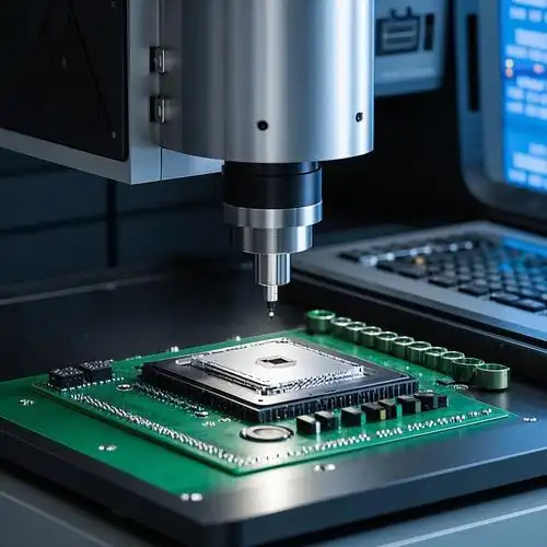
Working Principle of Laser Engraving PCB Boards
1) Laser Beam Generation and Focusing
The laser source within the equipment (e.g., CO₂ laser, fibre laser) emits a high-energy laser beam. This beam is directed through a focusing system (e.g., lenses, mirrors) to concentrate onto the PCB surface. Parameters such as laser power, frequency, and pulse width can be adjusted to control the beam’s energy and focal spot size, adapting to diverse engraving requirements.
2) Interaction Between Laser and PCB Materials
Upon striking the PCB surface, the laser energy is absorbed by the PCB materials (e.g., copper layer, substrate material) and converted into thermal energy. This thermal energy causes rapid temperature elevation in the irradiated localised area, inducing the following effects:
Copper Layer Removal: The laser locally heats the copper surface to high temperatures, causing it to melt or evaporate, thereby removing the copper layer to form circuit patterns.
Marking: High temperatures on the PCB surface induce chemical reactions (e.g., oxidation, carbonisation) that alter its colour, enabling the imprinting of markings, patterns, or text.
Cutting: The laser enables precise cutting along PCB edges to produce circuit boards of specific shapes or dimensions.
3) Heat-Affected Zone Control
As laser processing relies on localised heating, precise control of laser power, pulse frequency, and scanning speed is essential to minimise the heat-affected zone. This prevents material overheating or deformation, preserving the board’s dimensional accuracy and structural integrity.
4) Laser Scanning and Path Control
Laser engraving is typically achieved by controlling the laser head to scan along a predetermined path. During processing, the laser engraving machine automatically plans the path based on PCB design files (such as Gerber files), precisely directing the laser head’s movement to follow the circuit pattern’s trajectory, thereby completing the engraving or cutting.
Application Process of Laser Engraving PCB Boards
Copper Removal: Laser engraving is commonly employed to remove the copper layer from the PCB surface, forming the circuit pattern. By precisely controlling the laser beam’s heat and exposure time, the copper layer is effectively removed without damaging the substrate material. Laser engraving offers exceptional precision, making it suitable for intricate and minute circuit patterns.
Etching and Marking: Laser engraving can also be employed to etch identifiers, text, barcodes, QR codes, and similar markings onto PCB surfaces. Compared to traditional screen printing, laser marking offers superior durability and accommodates small-batch custom production requirements.
Cutting and Punching: Laser engraving is equally applicable for cutting or punching operations, particularly suited for fabricating complex-shaped PCBs or specialised applications requiring perforations. Laser drilling achieves higher precision than conventional methods, enabling micrometre-level apertures.
Advantages of laser engraving pcb boards:
High precision: Laser engraving achieves exceptional accuracy, making it suitable for intricate and minute circuit patterns.
Non-contact processing: The laser does not directly contact the circuit board during processing, eliminating errors caused by mechanical wear or contact.
Rapid processing: Compared to traditional chemical etching or drilling methods, laser engraving is significantly faster, making it ideal for rapid prototyping and small-batch production.
Environmentally friendly: Laser engraving does not utilise harmful chemicals, making it a more sustainable alternative to conventional chemical etching processes.
Disadvantages of Laser Engraving:
Higher cost: The capital expenditure and maintenance costs for laser engraving equipment are relatively high, potentially making it less economical than traditional methods for large-scale production.
Material-dependent: Different PCB materials (such as FR4, CEM-3, etc.) react differently to laser engraving, often requiring adjustments to laser power and speed to achieve optimal results.
Laser engraving PCB boards typically employs fibre lasers, CO₂ lasers, or ultraviolet lasers. These lasers possess distinct wavelengths and power levels, catering to different materials and processing requirements.
Fibre laser: Suited for high-precision machining, particularly engraving on metallic materials.
CO₂ laser: Ideal for processing non-metallic materials, though also applicable for engraving certain specific metals.
Ultraviolet laser: Suited for finer machining, especially within precision micro-machining applications.
Laser engraving PCB boards demonstrates unique advantages, notably in high precision, rapid processing, and environmental sustainability. Although it entails higher costs and stricter material requirements, ongoing technological advancements and increasing adoption will enable laser engraving to play a greater role across more sectors. This includes high-precision circuit board production, rapid prototyping, and personalised marking. Looking ahead, laser technology is expected to integrate with other manufacturing processes, further propelling the PCB industry towards greater efficiency and environmental responsibility.