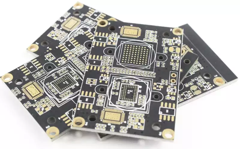
Against the backdrop of advancing radio frequency and microwave technologies such as 5G communications, satellite navigation, and radar detection, systems now demand higher standards for signal transmission stability, high-frequency performance, and interference resistance. Traditional PCB materials, such as FR-4, struggle to meet the demands of certain high-end applications due to significant high-frequency losses and limited dielectric stability. In contrast, ceramic PCBs offer lower high-frequency losses, stable dielectric properties, and superior thermal management capabilities. Consequently, they are increasingly being adopted in RF and microwave applications, playing an ever-growing role in communications, defence, and aerospace sectors.
Critical Requirements for Substrate Materials in RF and Microwave Circuits
RF and microwave circuits typically operate within the high-frequency range spanning hundreds of megahertz to tens of gigahertz. Characterised by short signal wavelengths and elevated frequencies, these circuits exhibit extreme sensitivity to minute variations in circuit parameters. Consequently, the performance demands placed upon substrate materials significantly exceed those of conventional digital or low-frequency circuits, with material properties often directly influencing the electrical performance and long-term stability of RF systems.
Under high-frequency conditions, the dielectric constant of substrate materials must exhibit excellent stability. This requires not only controllable numerical values but also minimal deviation during frequency variations and temperature fluctuations. Such stability is crucial for ensuring consistent transmission line impedance, accurate resonant frequencies, and stable phase characteristics. Excessive fluctuations in dielectric properties readily induce impedance mismatches and frequency drift, thereby increasing the complexity of system tuning and compensation.
Concurrently, the level of dielectric loss exerts a particularly direct influence on the performance of RF and microwave circuits. Elevated dielectric loss causes significant signal attenuation during transmission and introduces additional phase errors, thereby reducing system gain and signal-to-noise ratio. In high-power or long-link applications, loss issues further translate into heat accumulation, adversely affecting stable system operation.
As the power density and integration of RF components increase, the thermal conductivity of substrate materials has become an increasingly critical factor. Superior thermal conductivity facilitates the rapid dissipation of heat generated during device operation to heat sinks, mitigating localised temperature rises. This reduces the impact of thermal variations on electrical performance and extends the operational lifespan of both components and modules.
Furthermore, RF and microwave systems are frequently deployed in demanding environments such as communication base stations, radar installations, and aerospace applications. These prolonged operational conditions impose stringent requirements on substrate materials’ mechanical strength and thermal stability. Maintaining dimensional and performance stability under thermal cycling, vibration, or stress helps prevent circuit parameter drift and structural reliability degradation.
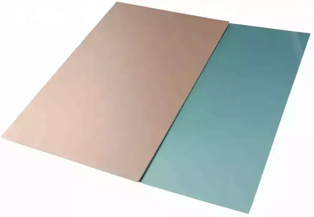
Material Properties of Ceramic PCBs:
Advantages in Dielectric Stability
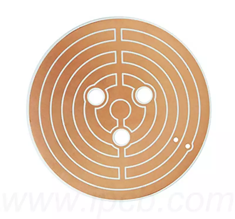
Ceramic materials exhibit remarkable dielectric stability, with minimal fluctuation in dielectric constant across broad frequency bands (e.g., DC to tens of GHz) and significantly lower dispersion effects than organic substrate materials. This property eliminates the need for frequency-specific parameter adjustments during circuit design, making it particularly suitable for RF structures demanding stringent impedance matching precision—such as filters and couplers—while substantially enhancing circuit consistency and repeatability.
Low Loss Properties Safeguarding Signal Integrity
The dielectric loss factor (Df) of ceramic substrates typically ranges from 0.001 to 0.002, representing merely one-tenth to one-twentieth that of conventional FR-4 organic materials. At microwave frequencies, this ultra-low loss characteristic substantially reduces both conductor and dielectric losses in transmission lines, minimising signal attenuation and phase distortion. This directly and critically enhances system gain, optimises signal-to-noise ratio (SNR), and lowers overall power consumption, making it particularly suitable for long-distance transmission or high-sensitivity reception scenarios.
Synergistic Optimisation of Thermal Conductivity and Insulation Properties
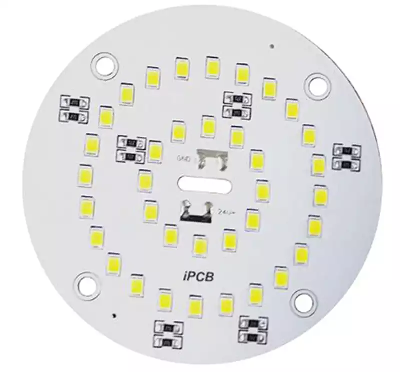
Ceramic materials simultaneously exhibit outstanding thermal conductivity (e.g., aluminium nitride reaches 170–230 W/m·K) and high volume resistivity (>10¹⁴ Ω·cm), fulfilling dual requirements for thermal management and electrical insulation. In high-power-density devices such as RF power amplifiers and T/R modules, ceramic substrates can directly serve as heat dissipation pathways, efficiently transferring heat generated by chips to cooling structures without requiring additional insulating layers. This simplifies manufacturing processes while avoiding thermal resistance increases caused by multi-layer structures, thereby ensuring reliable device operation in high-temperature environments.
Enhanced Environmental Adaptability
Ceramic substrates exhibit low water absorption (<0.01%), high mechanical strength (flexural strength 300–500 MPa), and radiation resistance. They withstand extreme temperatures (-180°C to +300°C), vibration shocks, and high-humidity environments, meeting long-term stability requirements for demanding applications like aerospace and automotive radar. This significantly reduces performance degradation risks from environmental factors.
The Role of Ceramic PCBs in Typical RF and Microwave Applications
At the practical application level, ceramic PCBs have been extensively deployed across diverse RF and microwave functional modules.
Within RF power amplifiers and microwave power modules, ceramic PCBs effectively reduce device junction temperatures through low thermal resistance structures, enhancing output stability and long-term reliability. Their favourable thermal expansion matching further mitigates solder joint fatigue and device failure risks.
In high-frequency filters, matching networks, and passive microwave components, ceramic PCBs maintain consistent circuit parameters across batches and operating conditions due to their stable dielectric properties, thereby enhancing system repeatability and debugging efficiency.
Within radar, satellite communications, and millimetre-wave modules, the dimensional stability and environmental adaptability of ceramic PCBs become particularly advantageous, meeting the combined demands of high-frequency operation, high reliability, and complex environmental applications.
Comprehensive Impact on System Design
From a system-level perspective, the incorporation of ceramic PCBs not only enhances the performance of individual components or modules but also introduces greater controllability in RF and microwave system design:
Facilitates more precise impedance design and signal consistency
Reduces frequency drift and performance fluctuations caused by temperature variations
Simplifies thermal management design to some extent, enhancing system integration
These characteristics confer long-term application value for ceramic PCBs in high-performance RF and microwave systems.
As RF and microwave systems advance towards higher frequencies, greater power density, and enhanced reliability, the role of substrate materials in system performance becomes increasingly prominent. Looking ahead, with the continued maturation of manufacturing processes and accumulation of application experience, ceramic PCBs are poised to provide stable support in more high-frequency, high-reliability scenarios, establishing themselves as a practically significant substrate choice in RF and microwave system design.