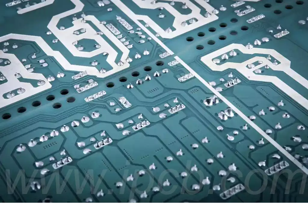
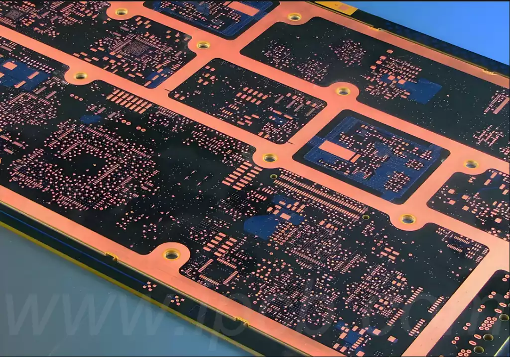
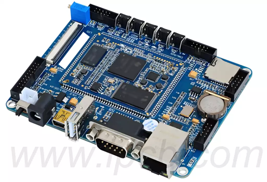
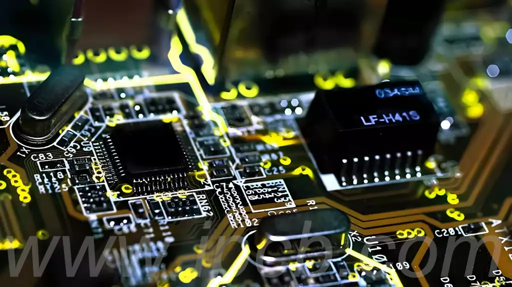
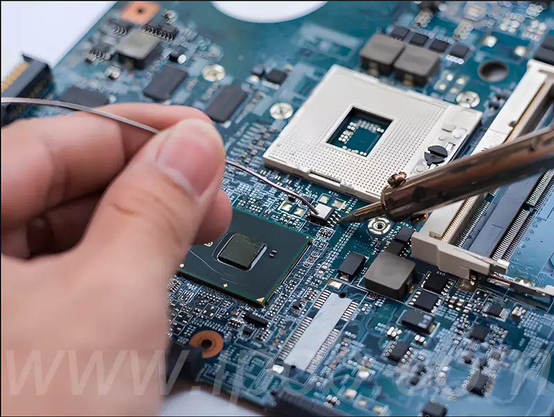
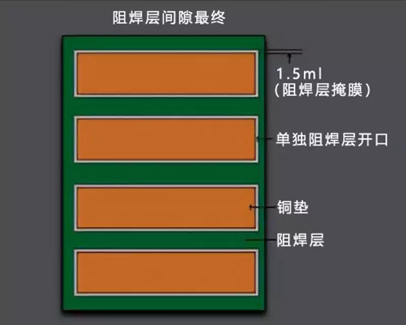
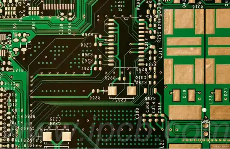
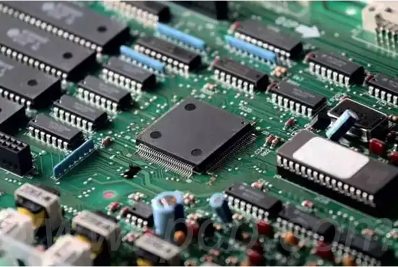
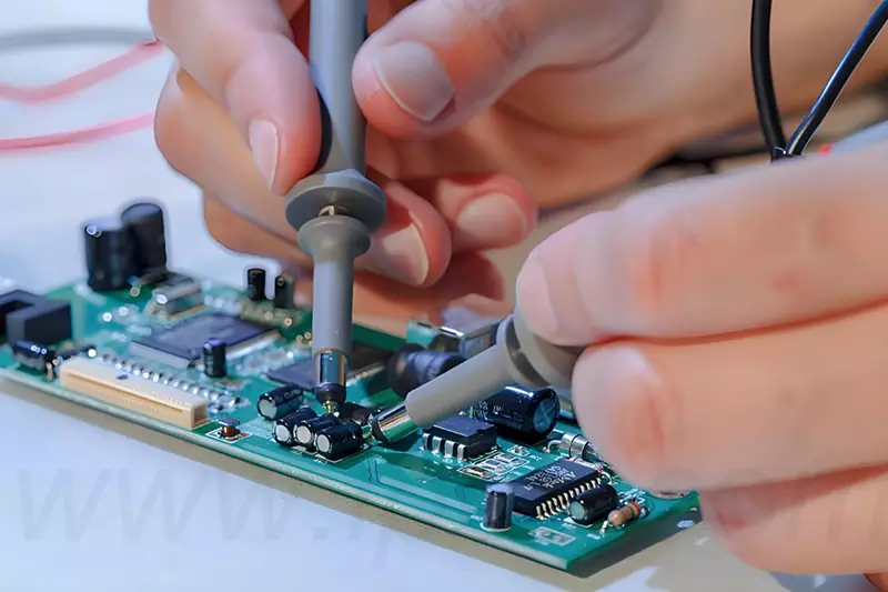
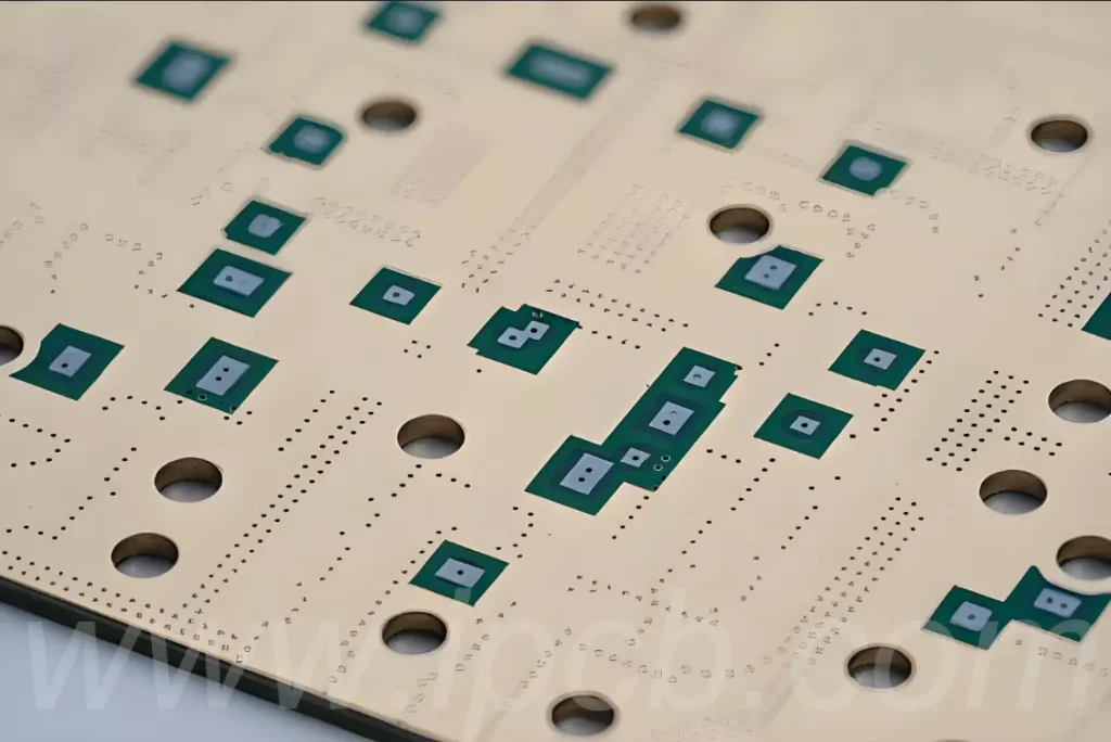
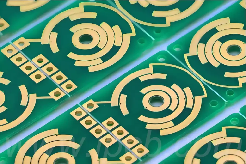
Electronic manufacturer

pcb layout rules

PCB layout rules and guidance

When designing a printed circuit board (PCB), following basic pcb layout rules is essential to ensure the functionality and performance of the circuit. The basic rules of PCB layout:1.According to the layout strategy of ‘major priority, complexity first’, i.e., the key unit circuits and core components should be arranged first.2.In the layout process, should refer […]

pcb edge plating

PCB Edge Plating Technology

PCB side plating, also known as pcb edge plating, is a copper plating that is applied from the top to the bottom surface of the board and along (at least) one of the peripheral edges. PCB edge plating is the process of allowing a metallised layer to extend up to the edge of the board

circuit card assembly testing

Importance of circuit card assembly testing

In the production process of electronic products, circuit card assembly testing is a crucial step, which is directly related to the performance and reliability of the product. Circuit card, as a carrier connecting various electronic components, the quality of its assembly directly affects the function of the whole system to achieve. Therefore, a reasonable assembly

custom pcb cost per unit

Custom pcb cost per unit impact factors

In modern electronic equipment manufacturing, the cost of printed circuit boards (PCBs) represents a significant portion of the total product cost. The custom pcb cost per unit fluctuates due to diverse market demands and technological developments. This article will analyse in detail the main factors affecting the custom pcb cost per unit. 1.Material CostThe material

circuit card assembly

Circuit Card Assembly Manufacturing Process

Circuit card assembly (CCA) is thin, flat board of dielectric material with conductive paths or tracks etched on their surface. In order to automate the production of CCAs, surface mount technology (SMT) and through-hole assembly machines are often used. Those responsible for the layout design and assembly of this form of manufacturing must have extensive

insulate metal substrate

Insulate Metal Substrate Design and Manufacturing

Insulate Metal Substrate, as a type of computer motherboard, aims to improve thermal efficiency and mechanical strength by applying metallisation to a thick substrate. It is also known as aluminium substrate, aluminium cladding or metal clad PCB (MC PCB), and even thermally conductive PCB (in fact, all PCBs are thermally conductive). Compared to the regular

insulate metal substrate

Innovative applications for insulate metal substrate

Insulate metal substrates are made using a unique insulating material that presses the copper foil of the circuit board to the metal substrate. The metal substrate is specially treated to increase adhesion and resilience, which allows the board to withstand the mechanical and thermal stresses of many applications. The insulating material is a special blend

Glass Substrate in Semiconductor

Role of Glass Substrate in Semiconductor

Semiconductor base material is an indispensable component in the development of contemporary advanced manufacturing, which is widely used in the production of various electronic devices such as transistors, light-emitting diodes and solar cells. In the manufacturing process of semiconductor products, selecting the right substrate is a crucial part of the process, as the quality of

pcb board etching

PCB Board Etching Technology Overview

PCB board to be retained on the part of the copper foil pre-plated layer of lead and tin resist layer, and then chemically corrode off the rest of the copper foil, known as etching. So, what are the types of PCB board etching and commonly used etching agents? 1.Types of etching graphic plating method: etching

printed circuit board switches

Printed Circuit Board Switches Selection

The printed circuit board switches are the components used to control the switching state of a circuit, also known as a switching circuit board or switch board. It usually consists of one or more triggers and controllers, and is used in circuits to control the on/off state of the circuit, thus acting as a switch

ceramic pcb materials

Types and properties of ceramic pcb materials

Ceramic pcb materials, with their excellent physical and chemical properties, are increasingly being used in electronics, aerospace, medical and energy applications. In this paper, we will discuss the properties of ceramic pcb materials, their preparation process and their wide range of applications. Currently, commonly used ceramic substrate materials for electronic packaging include alumina (Al2O3), aluminium

water temp pcb

Advantages and applications of water temp pcb

A water temp pcb is a circuit assembly specifically designed to monitor and control the temperature of water. Its core function is to ensure that various water-related systems operate efficiently and safely within a set temperature range. Such circuit boards typically contain several key components to enable precise management and regulation of water temperature. ComponentsTemperature

solder beads

Causes and countermeasures of solder beads

Solder beads refer to the small spherical or dotted solder that appears on the pads or on the metal layer on the backside after SMT circuit board assembly. The diameter of the bead is roughly between 0.2mm and 0.4mm, but there are also more than this range, mainly concentrated around the chip resistive components. The

Types and applications of pcb connectors

PCB connector is a key component used in electronic equipment to achieve circuit connection and signal transmission, plays a key role in connecting circuit boards and external devices, and achieving signal and current transmission. In modern electronic products, the design and selection of connectors are critical to the performance, stability and reliability of the entire

hf board

HF board characteristics and layout points

HF board refers to special circuit boards with high electromagnetic frequency, which are used in the field of high frequency (frequency greater than 300MHZ or wavelength less than 1 metre) and microwave (frequency greater than 3GHZ or wavelength less than 0.1 metre), and the circuit boards are produced by using some of the processes of

printed circuit board rf chip

Printed Circuit Board RF Chip

Printed circuit board radio frequency (RF) chip, also known as printed circuit board rf chip, is the core components in the field of wireless communications and are responsible for converting RF signals to digital signals or digital signals to RF signals for wireless transmission of information. RF chips are usually composed of several key parts,

double sided PCB board

Double sided PCB board characteristics and material

A double sided PCB board (or 2-layer PCB) is a printed circuit board coated with copper on both sides, top and bottom. There is an insulating layer in the middle. To use circuits on both sides, there must be a proper circuit connection between the two sides. The ‘bridge’ between such circuits is called a

Bluetooth pcb board

Bluetooth pcb board design and application

Bluetooth pcb board is a key electronic component that plays an important role in modern technology. Bluetooth pcb board is a wireless communication technology that transmits data and information through wireless signals. It uses specific frequencies and protocols for communication and allows interconnectivity between devices. The output of Bluetooth circuit boards is to transmit data

pcb warping

Analysis and prevention of PCB warping and twisting

In printed circuit board (PCB) manufacturing, pcb warping and twists are often seen as the top defects in nonconformities, which often stems from a lack of in-depth understanding of their causes. Many novice inspectors incorrectly regard perfectly flat, rigid boards as the norm, but in reality, understanding the root causes of PCB warping and twisting

layers of a pcb

Layers of a pcb and structure

Layers of a pcb is the copper layer, PCB is made of copper layer + substrate compression and become, in addition to a single panel is a layer of copper, double-sided above the board is an even number of pcb layers. Components are soldered on the outermost layer, the other layers play a role in

PCB button

Exploring the optimisation of pcb button materials

PCB buttons are everywhere we live and work, from mobile phones and TV remotes to computer keyboards, keys are an important medium of interaction between us and our devices. PCB buttons are switching elements embedded in a printed circuit board (PCB), typically used to receive input commands from the user.When the user presses the button,

signal Integrity

What is signal integrity?

In modern electronic equipment, high-frequency and high-speed performance is gradually becoming the industry standard. People have higher requirements for the speed, precision and reliability of various electronic products, which makes the issue of signal integrity in PCB (Printed Circuit Board) design particularly important. When we talk about high-frequency, high-speed SOCKETs, signal integrity is not only

pcba

Importance of PCB Assembly and Design Tips

PCB assembly is the process of combining a circuit board with other electronic components (e.g., connectors, housings, heat sinks, etc.) to be embedded in the final product. PCB Assembly Design Tips1.Pay attention to the gap between components One of the most common issues raised by PCB Layout gurus: component-to-component spacing. Two components that are too

pcb line width

What is PCB trace width?

What is trace width in PCB?PCB Trace width is the width of the wires or alignments on a circuit board.It is usually measured in millimeters or inches, e.g., 0.2mm, 8mil, etc. The choice of line width depends on factors such as the circuit’s power requirements, signal frequency, impedance control and manufacturing process requirements. Depending on

Scroll to Top