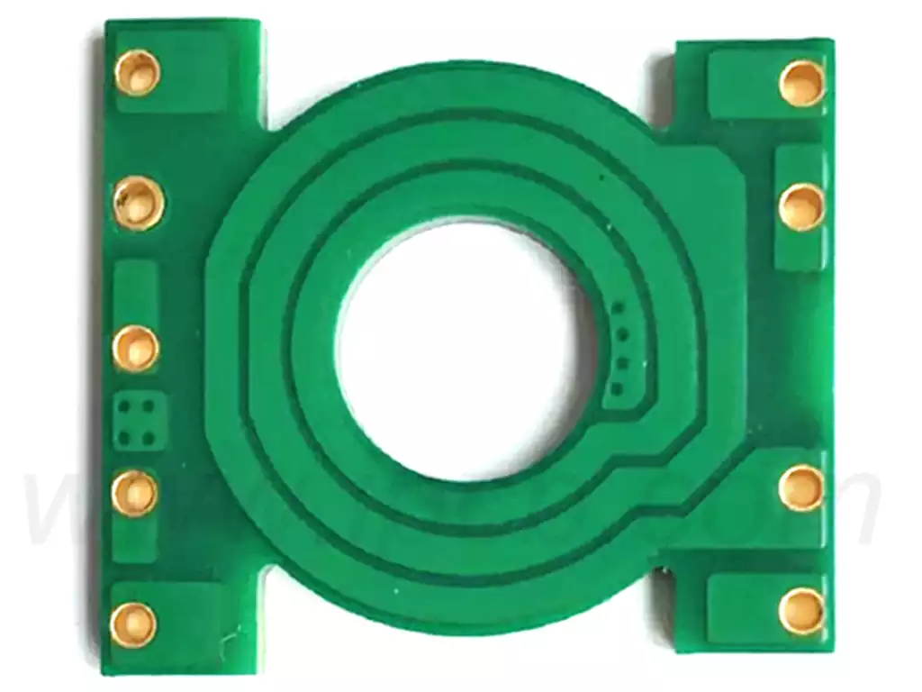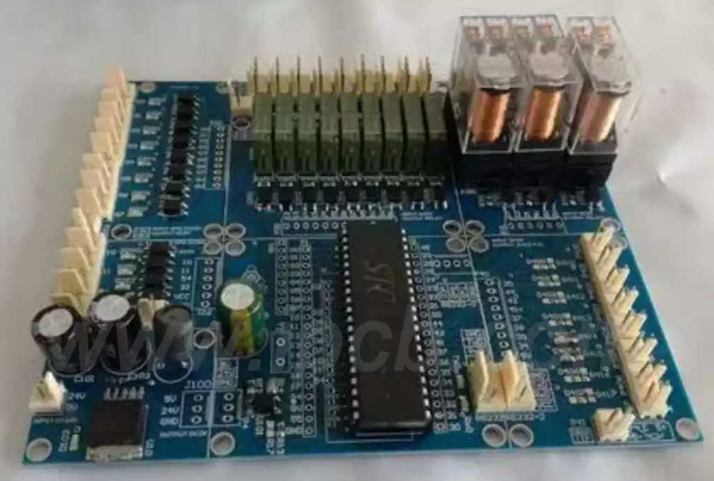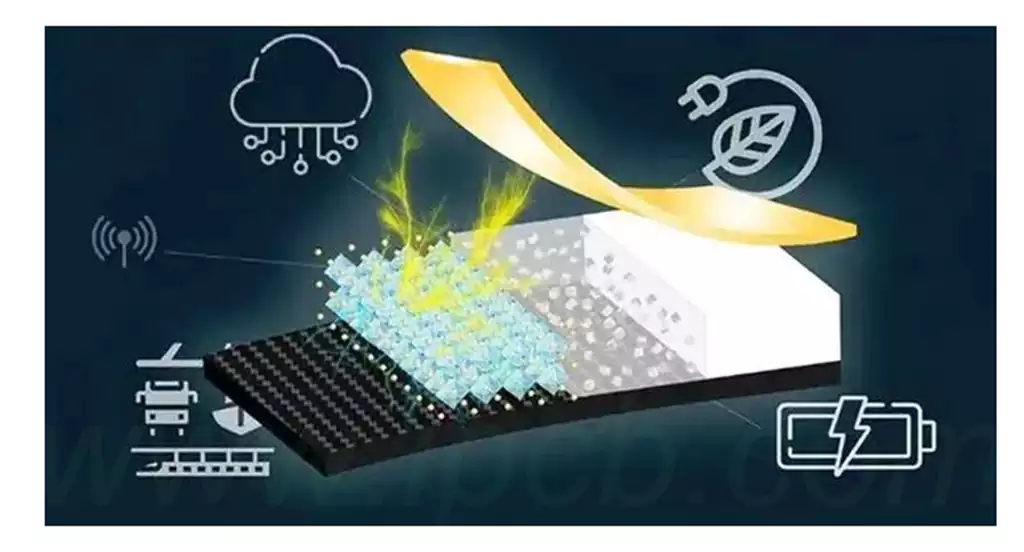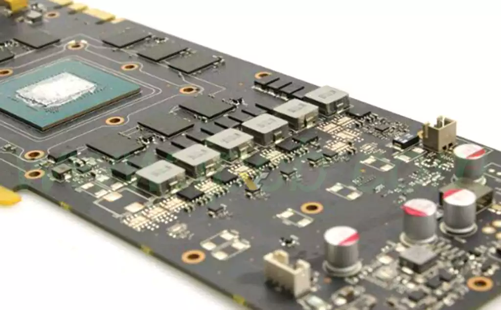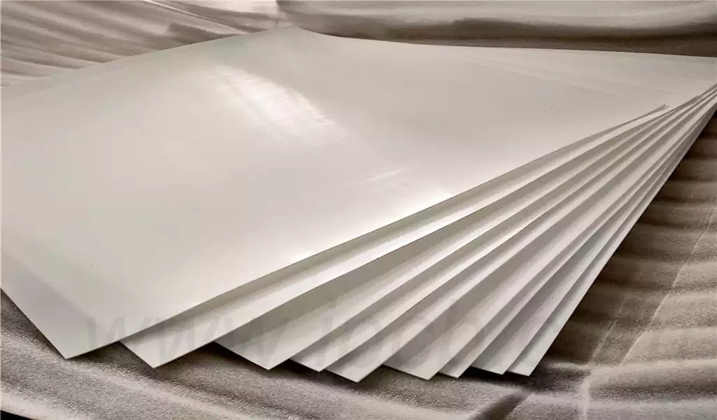
PTFE plate characterization and application
PTFE plate, i.e. polytetrafluoroethylene plate, is a polymer material made of polymerized tetrafluoroethylene monomer. Its unique molecular structure makes it a material with excellent corrosion resistance, high and low temperature resistance, and non-adhesive properties, often referred to as the “king of plastics”.PTFE plate can be made through a variety of processing methods, including molding, extrusion […]