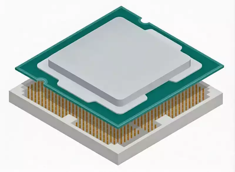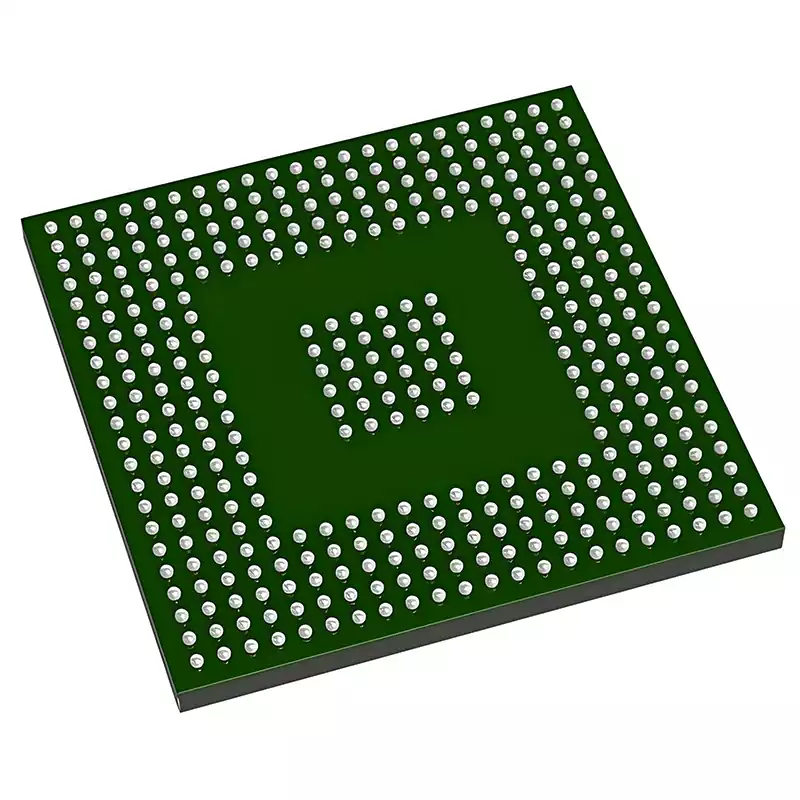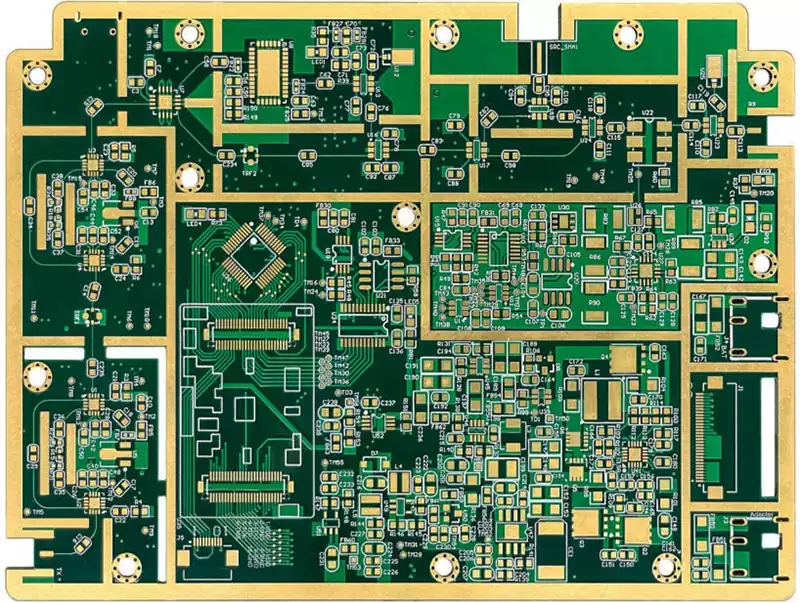
Key Considerations for Design for Manufacturability in High-Density BGA PCBs
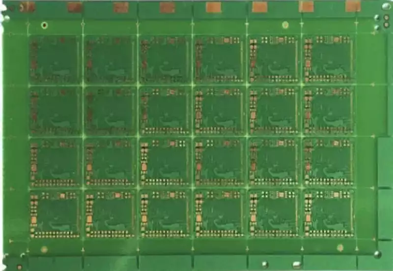
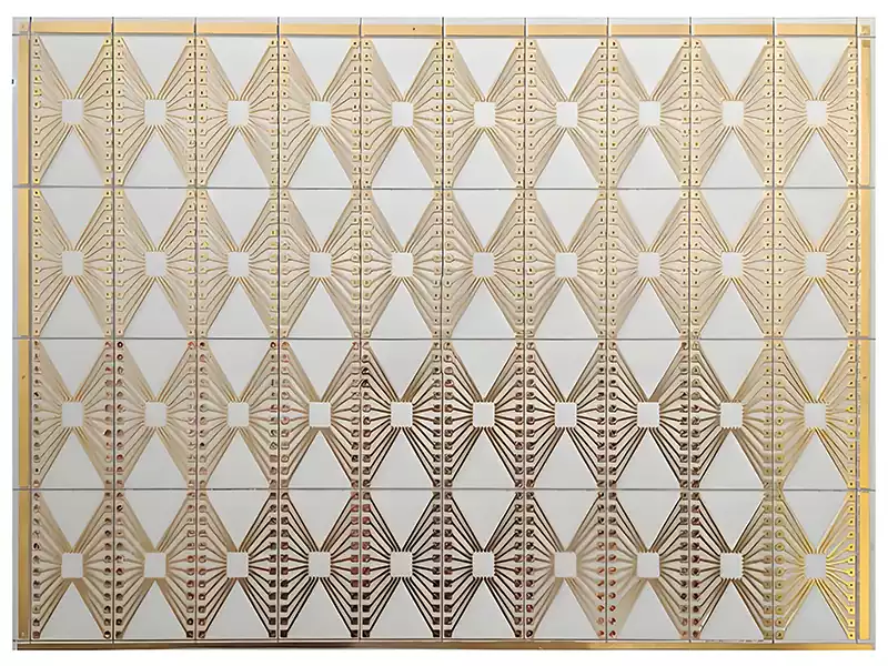
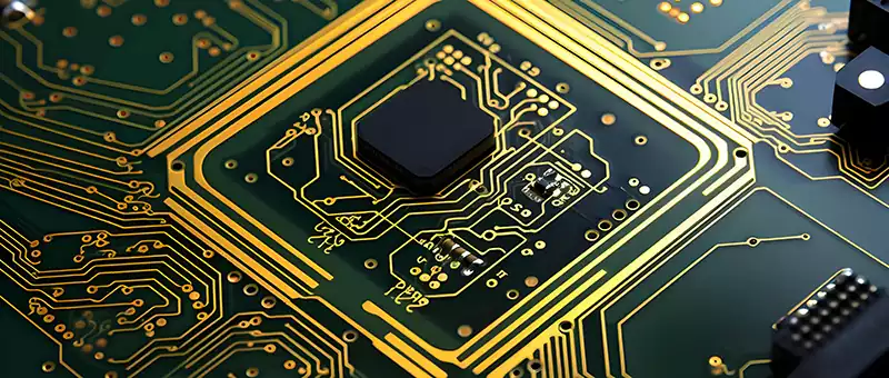
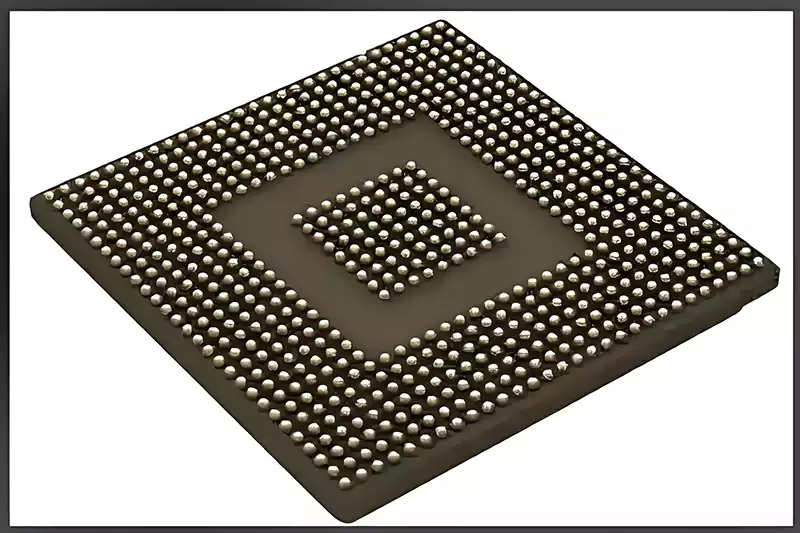
As the functionality of electronic products continues to evolve, the number of components mounted on PCBs is constantly increasing, component pin pitches are becoming increasingly fine, and circuit design is gradually shifting from conventional wide-pitch surface-mount technology to ultra-fine-pitch BGA layouts. Thanks to their high-density integration, excellent electrical performance and thermal management advantages, BGA (Ball […]