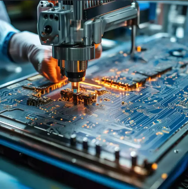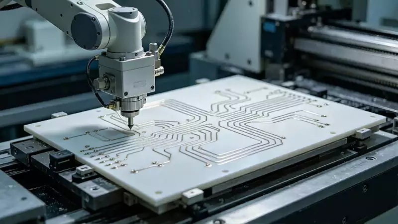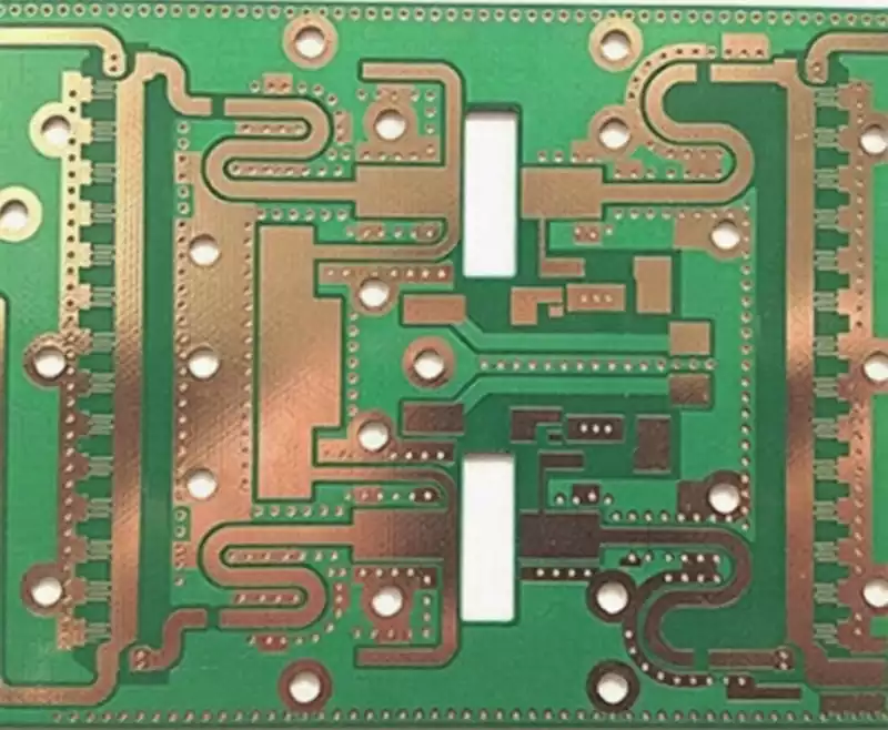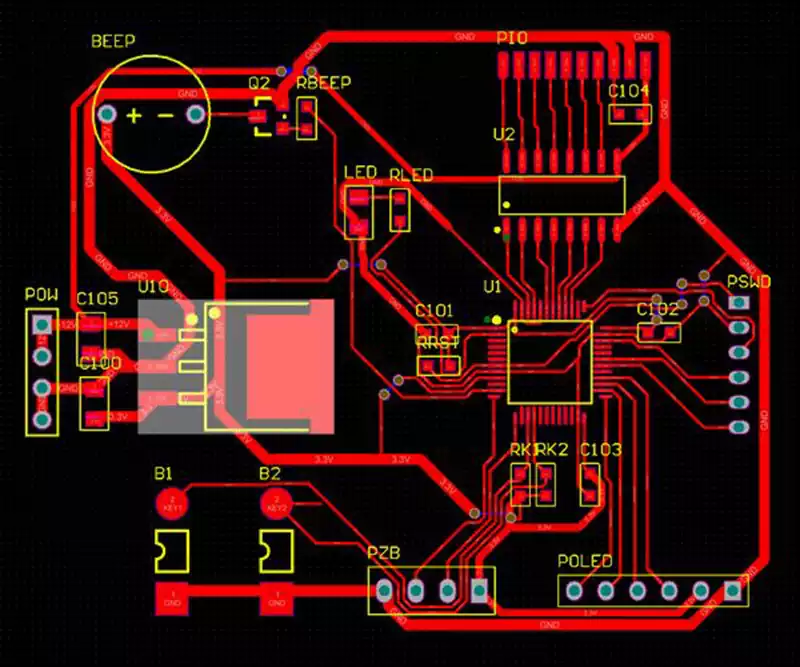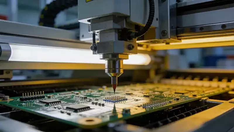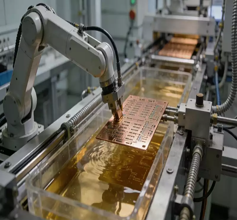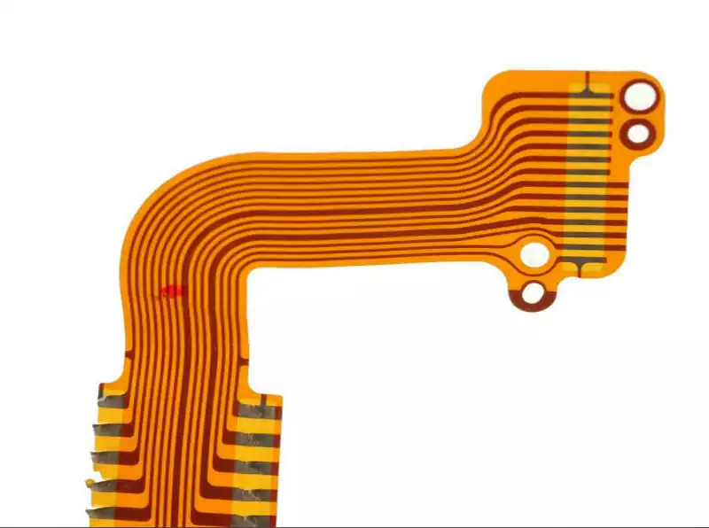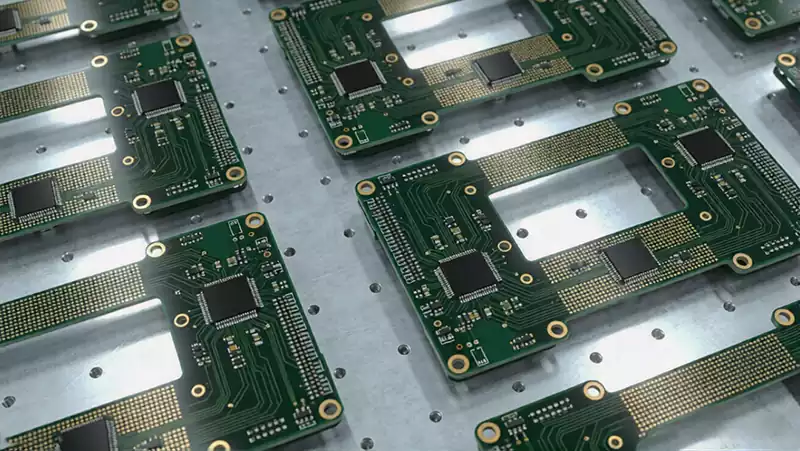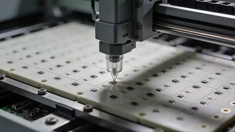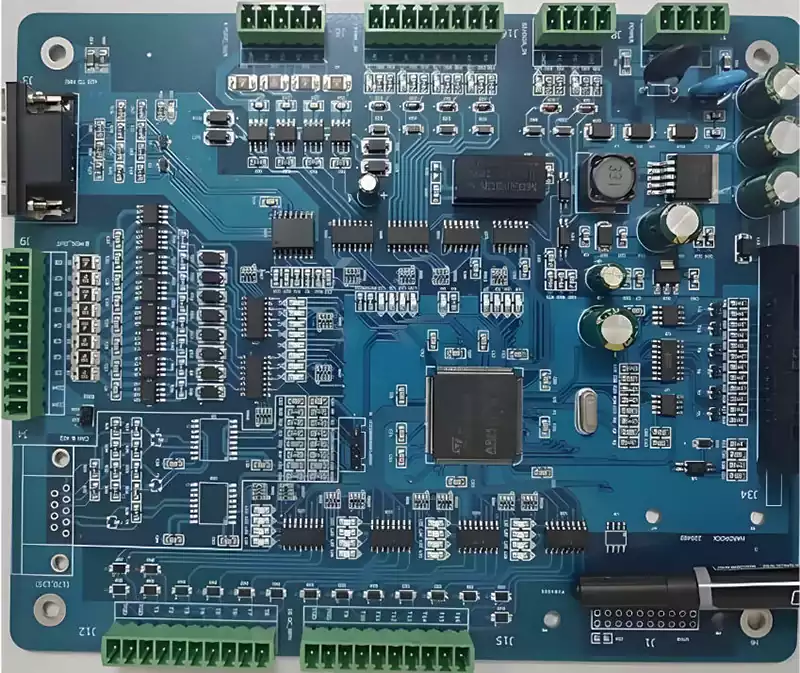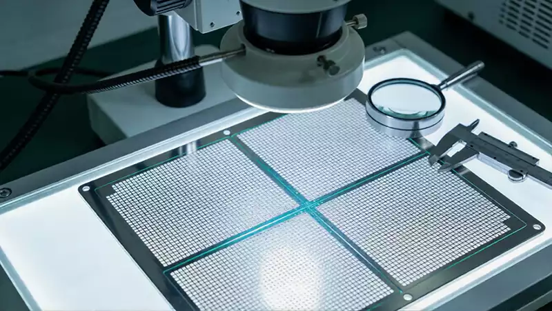
Comparison of Ceramic PCB Manufacturing Processes: Subtractive and Additive Methods
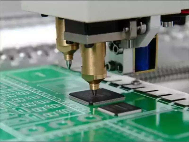
Every improvement in the precision of flexible circuit formation drives the expansion of ceramic pcb into high-end applications such as 5G communications, medical electronics and aerospace. As the two core processes in the PCB manufacturing industry, subtractive and additive methods are not mutually exclusive; rather, they form a complementary and symbiotic technological landscape centred on […]