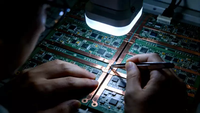
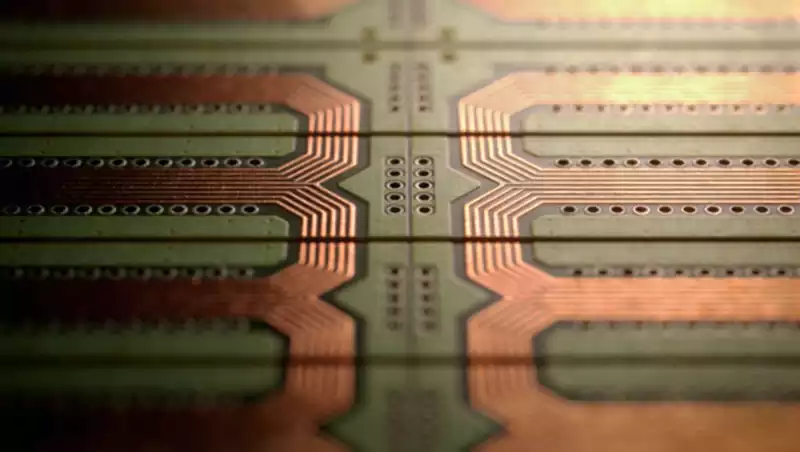
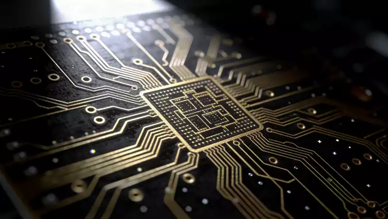
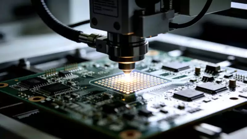
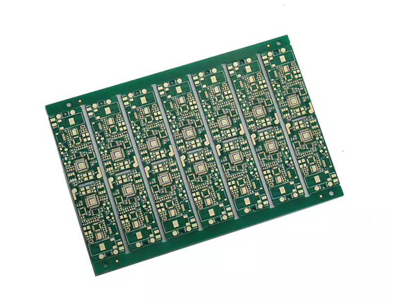
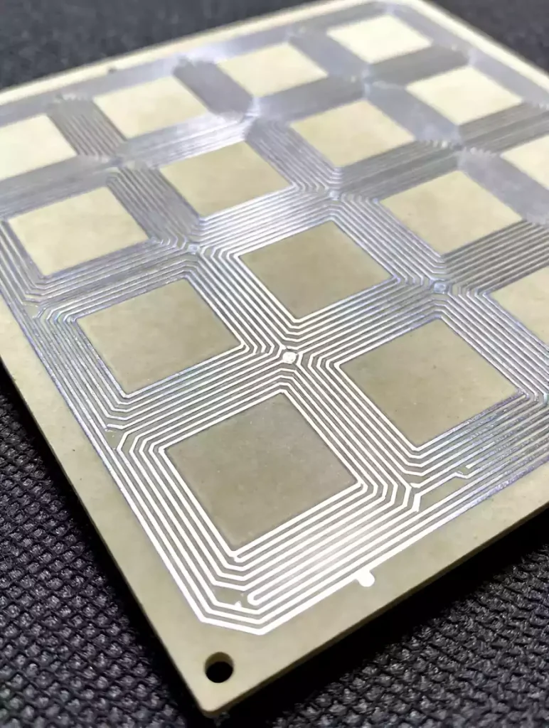
Electronic manufacturer

RF microwave PCB

Key Considerations for RF Microwave PCB Design and Application

PCB High Frequency Board (RF Microwave PCB) is a special type of circuit boards used to process signals at higher electromagnetic frequencies. This type of board is commonly used in high frequency (frequencies greater than 300MHz or wavelengths less than 1 metre) and microwave (frequencies greater than 3GHz or wavelengths less than 0.1 metre) applications, […]

computer pcb

Computer pcb technology development and application

The computer pcb is an important electronic component that is widely used in various electronic devices such as computers, mobile phones, TVs and so on. It is the core component of these devices, responsible for connecting and coordinating the work of various electronic components. The circuits on the motherboard are precisely designed and laid out

peelable solder mask

Application areas and functions of peelable solder mask pcb

A peelable solder mask PCB is a printed circuit board with a peelable solder mask (temporary solder resist) that protects certain areas during surface preparation or assembly. That is, sometimes a printed circuit board needs to have selected areas of the board protected from solder flow onto contacts, terminals and plated through holes (PTH) during

breakout board

Materials and functions of breakout board

A breakout board, called both an adapter board and a breakout board, is a board-like device used to connect, convert, or extend the functionality of electronic equipment. It can establish a connection between different devices or components to achieve signal transmission, conversion or processing. Adapter boards are widely used in a variety of electronic equipment,

exposed copper on pcb

Exposed copper on pcb causes harm and repair methods

Exposed copper on pcb refers to the surface of the circuit board part of the copper foil is processed to remove the exposed place called exposed copper, also known as exposed copper over the holes, exposed copper heat dissipation, and so on. The PCB exposed copper is often used to strengthen the circuit board structure,

alkaline etching

Alkaline etching technology for circuit boards

Alkaline etching solution for circuit boards, also known as passivation solution, is one of the widely used chemical etching solutions in the electronics industry for removing unwanted copper materials from circuit boards, and then generating a protective layer on the surface to protect the circuits on the boards from corrosion. The principle of action of

PCB board copper thickness

PCB board copper thickness and design guidelines

PCB board copper thicknesses are generally classified as 1oz (35μm), 2oz (70μm) and 3oz (105μm). Of course, the copper thickness depends on the type of board you are making. Copper thickness for switching power supplies with high currents is 2oz. for signal transmission, usually, 1oz is sufficient. Normal double-sided boards are 1oz. Multilayer circuit boards

bluetooth pcba

Bluetooth pcba board application areas and development

Bluetooth Data Module is a PCBA board with integrated Bluetooth functionality for short-range wireless communication. By integrating the chip and peripheral hardware circuits onto the PCB and developing inbuilt programs to implement the Bluetooth function, the module is capable of data transmission and networking with MCU controlled devices. It is widely used in the fields

semiconductor packaging

What is semiconductor packaging?

What is semiconductor packaging? Semiconductor Packaging is the process of processing a tested wafer into an individual chip according to the product model and functional requirements. The purpose of traditional packaging is to fix, lead and seal the cut chip, but with the advent of the post-Moore’s Law era, more and more steps that need

hdi pcb

Types and cost of hdi pcb

HDI PCB definition, High Density Interconnect Board, is a circuit board with high line distribution density using micro-blind/buried hole technology. It is able to achieve higher line density and finer wiring in limited space to meet the demand for miniaturisation, high performance and high reliability of modern electronic products. In the field of pcb board,

thermistor

Application and Manufacturing of Thermistors in Circuit Boards

On a circuit board, RT usually stands for Thermistor, a component that is extremely sensitive to temperature. The resistance value of a thermistor changes significantly with temperature, so by measuring its resistance value, we can accurately deduce the current ambient temperature. This characteristic makes thermistors play a vital role in circuit functions such as temperature

pcb test point

PCB Test Point Layout

PCB test points may look like just some pads or exposed copper skins, but their role in the entire production, debugging, testing and repair process is very critical. If the test points are not reasonably arranged, it will lead to difficult to test the circuit board, debugging time becomes longer, the difficulty of rework increases,

transparent flexible PCB

Future challenges and application for transparent flexible pcb

A transparent flexible PCB is a pcb board that can be bent and has a certain degree of flexibility without affecting its functionality. It is made of flexible materials such as polyimide or polyester film, allowing for compact circuit connections in a given space. Transparent flex pcb is lightweight and durable. It is this property

flexible circuit board

Key points and strategies for soldering flexible circuit board

FPC flexible circuit board is widely used in modern electronic products due to their thin, lightweight and bendable characteristics. However, its unique physical properties also bring many challenges to the welding process, requiring fine process control and specialised coping strategies. Flexible circuit boards in the welding process should pay attention to: Quality inspection is a

flex board

Deformation and Delamination Prevention in Flex Board Manufacturing

In the production of flex board, material deformation and delamination are important factors affecting product quality. In order to avoid such problems, the following detailed coping strategies can be adopted: Substrate selectionThe choice of material directly determines the basic bending performance of flex board. In terms of substrates, polyimide (PI) and polyester (PET) are commonly

high speed digital pcb

Key considerations and applications for high speed digital pcb

High speed digital pcb is circuit boards that can support high speed digital signal transmission, and are usually used in scenarios where the frequency of digital logic circuits reaches or exceeds 45MHz-50MHz, or where the delay of digital signals in circuits on the transmission line is greater than 1/2 rise time. Compared to traditional analogue

leadless chip carrier

Differences between leadless chip carrier and leaded chips

Leadless chip carrier refers to a chip substrate material that does not contain lead. Traditional chip carriers often use leaded materials because leaded materials have high plasticity and are easy to process during manufacturing, but leaded chips are harmful to the environment and the human body. Leadless chip carrier is widely used in the manufacture

pcb board assembly

Common defects in pcb board assembly processing

PCB board assembly processing, there may be a variety of defects, these defects can be categorised as the following major aspects, designed to improve product quality and reduce the defective rate. Welding defectsWelding is a key part of PCB board assembly processing, common welding defects include: False soldering (Dry Joints/Cold Solder): refers to incomplete solder

AMB ceramic substrate

Technology and Challenges of AMB Ceramic substrate

Ceramic substrate in accordance with the process points there are many kinds of, in addition to direct bonding copper (DBC) method, direct copper plating (DPC) method, laser activated metal (LAM) method, low-temperature co-fired ceramics (LTCC), high-temperature co-fired ceramics (HTCC) in addition to the AMB method of the technology that currently attracts much attention, that is,

chipset

What is a chipset and what does it do?

What is a chipset? A chipset is a processor that consists of multiple chips. Each chip in a chipset may be produced by a different manufacturer. These individual chipsets are combined together to form a processor using a complex connection system. Chipset processors can take advantage of the latest chip manufacturing technology to reduce the

ceramic substrates

Comparison of ceramic substrate and normal pcb

Ceramic substrates and PCBs play an important role in the electronics industry, each with unique material properties, manufacturing processes and application areas. Ceramic substrate is a ceramic material made of electronic substrates, belonging to the inorganic materials, usually with alumina (Al2O3), aluminium nitride (AlN) and silicon nitride (Si3N4) as the main component, ceramic substrate has

dip

What is dual inline package?

What is dual inline package? Dual inline package (DIP) is a type of integrated circuit package whose main feature is that the integrated circuit chip is mounted on two parallel rows of metal pins. This type of package is simple, easy to produce and maintain, so it is widely used in the electronics industry. Dual

ball grid array socket

Production considerations for ball grid array socket design

The ball grid array socket is an adapter that allows for pluggable mounting without directly soldering BGA-packaged integrated circuits (ICs) to the test substrate. By connecting the solder balls of the IC to the pads of the test substrate via the BGA socket, the risk of poor contact (e.g. open or short circuit) and IC

camera pcb board

Camera pcb board design

The design layout of a camera pcb board is a central aspect of ensuring camera performance, reliability and stability. An optimised layout can effectively reduce signal interference, improve signal integrity, and improve thermal management. Camera PCB Board Wiring GuideThe LVCMOS signal alignment needs to be away from the differential lines to prevent the LVCMOS line

Scroll to Top