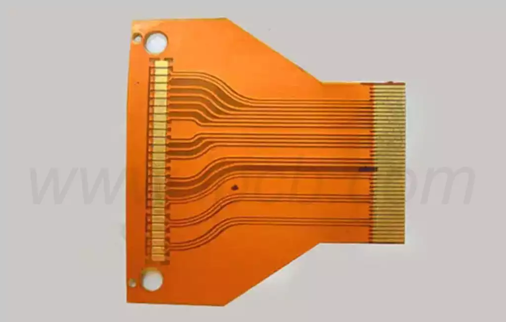
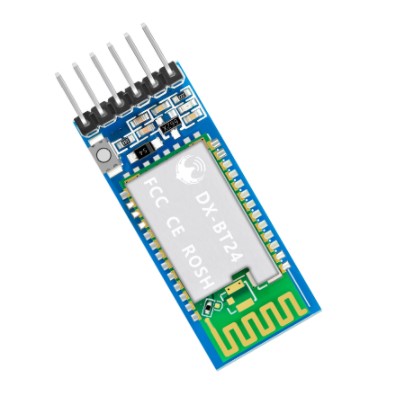
What is a Bluetooth module?Bluetooth module is a kind of integrated bluetooth pcb board, mainly used for wireless network communication, according to the function can be divided into the classic bluetooth module, low power bluetooth module and dual-mode high-speed bluetooth module.
The role of the bluetooth module is simply to replace the wired connection with a wireless connection,the fixed and mobile information equipment to form a personal local area network, to achieve low-cost wireless interconnect communication between devices.
There are several key aspects that need to be covered to understand the principles of Bluetooth pcb board. The following are some of the key aspects:
- Bluetooth module integration
Bluetooth module: Bluetooth devices usually use specialized Bluetooth chips (modules), such as Nordic Semiconductor, Qualcomm, Texas Instruments and other companies. These modules include the Bluetooth protocol stack and radio frequency (RF) circuitry.
Pin Connection: Ensure that the Bluetooth module’s power, ground, and signal pins are properly connected. - Power Management
Power supply stability: Bluetooth modules are sensitive to power supply noise. A stable power supply needs to be designed, and a low noise linear regulator or DC-DC converter may be used.
Decoupling capacitors: Add decoupling capacitors near the power supply pins to minimize the impact of power supply noise on the module. - Signal Integrity
Signal line layout: Signal lines (e.g. UART, SPI or I2C interface) should be as short and straight as possible to avoid crossover and interference.
Ground design: Use a continuous ground plane to reduce ground impedance and prevent signal loop interference. - RF Design
Antenna Design: Bluetooth devices require a proper antenna design. Common antenna types include printed antennas, external antennas, and helical antennas.
Antenna Matching: Ensure impedance matching between the antenna and module to maximize transmission efficiency. A matching network usually needs to be designed on the PCB. - Interference Management
RF Interference (EMI): Avoid interference from Bluetooth modules and other high frequency components. Maintain proper distance between high-frequency wires and sensitive components and use shielding.
EMC design: Consider electromagnetic compatibility when designing and make sure the PCB design complies with relevant standards (e.g. FCC, CE certification). - PCB Layout
Layout rules: Follow RF design rules, such as shortest signal paths, avoiding sharp corners and loops.
Multi-layer boards: Usually, bluetooth pcb boards are designed using multi-layer boards, where one layer is dedicated as ground plane to reduce noise. - Software and Firmware
Protocol Stack: Bluetooth modules are usually required to run a specific protocol stack such as Bluetooth Classic or Bluetooth Low Energy (BLE).
Drivers: Ensure that appropriate drivers are developed or configured to support the functionality of the Bluetooth module. - Testing and Verification
Signal testing: Use tools such as network analyzers and oscilloscopes to test signal quality and power stability.
Functional test: Verify the actual working of the Bluetooth module, such as pairing and communication stability.
Example circuit design basic connection diagram
Power supply: VCC pin is connected to the output of the voltage regulator, and GND pin is connected to ground.
Data interface: connected to the UART/SPI/I2C interface of the microcontroller.
Antenna interface: connects to the RF antenna on the PCB, usually with a matching network.
Antenna design schematic:
Printed Antenna: Microstrip line antenna designed on the PCB.
External antenna: connected to an external antenna via RF connector.
These design principles and details will help you successfully design a Bluetooth pcb board. Let me know if you need specific design tool or software recommendations, or have other specific questions!
Design Considerations
Bluetooth pcb board design guide
The Bluetooth PCB design process must consider a variety of requirements. Here, we are referring to the board that the BT module will connect to. Below, we will take you through the project requirements, which briefly include the following:
Bluetooth device selection
Material selection and stacking
Bluetooth PCB module selection
Circuit design and layout
- Bluetooth device selection
Determine whether you need low or high energy (classic) transmitters and receivers. “Low energy” is the latest development in Bluetooth technology. It provides greater flexibility in what you can accomplish with your device.
Higher energy (classic Bluetooth) types allow you to transmit more data but consume more power. Application limitations must also be considered when choosing between high-energy and low-energy devices.
Low Power vs. High Power Bluetooth
Choose Classic if your application involves streaming audio and a wide range of other data needs
Choose Low Power Bluetooth if the device is a location detection device or sensor messaging transmitter
Application Limitations
If your device will be operating in high EMI conditions as with nearby wireless devices, use lower speed, high power Bluetooth to minimize signal loss.
Also, if there are many obstacles in the operating environment, such as human bodies or metal objects
Most BT devices are portable. Be sure to keep this in mind when deciding on board size! - Module selection
Using pre-certified modules or BT PCBAs eliminates all the hard work of designing RF circuits. A variety of modules are available in different sizes. To select the type that suits your needs, consider the following factors:
Module version
Bluetooth 5.0 and its various upgrades (5.1, 5.2, 5.3 and 5.4) offer faster speeds and a wider signal range
Select the version that best suits your device’s needs based on your application requirements
Module size
Choose the chip size that fits the space constraints of your equipment
SMD chips save you space, so choose them if your board space is limited.
Sensing Range
Various modules offer different sensing ranges, from a few meters to 100 meters or more.
A wider range gives you more options for use.
Data Transfer Rate
Again, your choice depends on the usage requirements of your device.
Choose the module that can handle the data transfer rate of your device or application.
Voltage range
You can choose from a variety of operating voltages, with most modules in the 3V range.
Choose the lower voltage range to make board design requirements easier.
- Circuit Design and Layout
Proper placement of RF and other components reduces interference. Proper placement also reduces the length of the alignment, thus minimizing noise from coupling. On the other hand, optimized routing prevents crosstalk and maximizes signal quality.
Component Placement
Optimize component placement to shorten the alignment during the design process
Place the Bluetooth module close to the antenna and its connector.
Ensure proper clearance around the module and antenna
Routing
Keep high power or RF alignments short to reduce parasitic capacitance and crosstalk, also separate digital and RF alignments, and widen ground and power alignments.
Power Distribution and Grounding
Ensure an efficient power distribution network to avoid voltage fluctuations, and for thermal management, use heat sinks and select low-power components.
Depending on your motherboard or device type, you may also include heat sinks, use grounding layers between signal layers to avoid crosstalk
Impedance control, maintaining controlled impedance to avoid signal loss due to impedance mismatch. To do this, ensure proper alignment width and spacing, and use EMI shielding (such as cans and ferrite beads) to minimize interference.
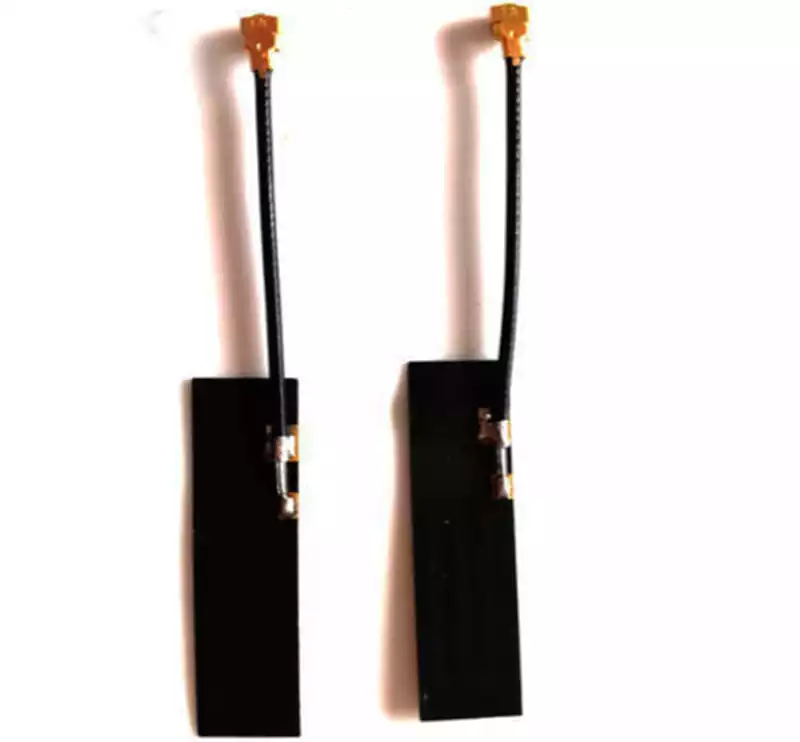
Antenna Design
Your module may or may not be equipped with an integrated Bluetooth antenna!
If not, create one on the bluetooth pcb board and make sure it meets the module’s certification specifications
Choose the right antenna design and type for your device and board size
Your options include chip, alignment and external PCB antennas
For smaller Bluetooth devices, we recommend a meandering inverted F trace antenna
Keep the antenna away from components and signal or power transmission lines to avoid signal degradation.
- Testing and Design Verification
After completing the Bluetooth PCB design steps, you can test it to make sure it works as expected. These tests include signal integrity tests, EMI and EMC tests, and antenna performance tests.
After verifying your Bluetooth PCB design, you can send it in the following form: Gerber file to your preferred manufacturer for production. The manufacturer will evaluate the design and provide further advice before manufacturing the board.
Material Selection and Stacking
Ask yourself questions like: do I need a flexible PCB or a rigid PCB and what is the allowable operating temperature? Also determine the stacking as this may affect signal quality, power flow and thermal performance.
Material Options
For flexible boards, your options include polyimide and PTFE
If you want the board to be rigid, you can use the more common FR4 or Roger
Choose low dielectric constant materials such as Rogers and Isola to avoid signal quality problems.
Number of Layers on a Bluetooth PCB
Number of layers will vary depending on signal isolation and power/ground decoupling requirements
More layers means more design flexibility and better chance of avoiding problems
Consider a minimum of 4 and a maximum of 6 layers for optimal routing and RF shielding
The future of Bluetooth pcb boards will be driven by technological advances and market demand, and several trends are likely to emerge:
- Higher data transfer speeds
As technology advances, Bluetooth standards continue to improve. For example, Bluetooth version 5.0 and above already offers higher data transfer speeds and greater data bandwidth. Future Bluetooth PCB designs may continue to support higher speed data transfer to meet the demand for high-speed data streaming, such as HD video streaming or real-time data processing. - Lower Power Consumption
Bluetooth Low Energy (BLE) has been widely used in many applications. Future Bluetooth pcb boards may further optimize power consumption to support longer battery life and higher energy efficiency. Technological advances may lead to more efficient power management and smarter power control strategies. - Higher Integration
Increased integration can reduce system cost and footprint while improving system reliability. Future Bluetooth pcb boards may integrate more functions, such as sensors, processors, and memories, to simplify design and reduce cost. For example, there may be all-in-one modules that integrate Bluetooth, Wi-Fi, GPS and other functions. - Smarter devices
The rapid development of smart devices and the Internet of Things (IoT) will drive the development of Bluetooth technology. Future Bluetooth pcb boards are likely to be smarter, with stronger data processing capabilities and richer functionality, such as intelligent algorithms and machine learning processing. - Stronger security
As the application of bluetooth technology expands, security becomes more and more important. Future Bluetooth PCB designs will likely focus more on security, including stronger encryption algorithms and security protocols to prevent data leakage and unauthorized access. - Wider application scenarios
Bluetooth technology will continue to expand into more application scenarios, including:
Healthcare: smart health monitoring devices, wearable devices, etc.
Smart home: smart lights, door locks, home appliances, etc.
Industrial automation: industrial monitoring, asset tracking, smart sensors, etc. - Higher compatibility and interoperability
The evolution of Bluetooth standards will lead to greater compatibility and interoperability between devices. Future Bluetooth PCB designs will need to support multiple Bluetooth standards to ensure compatibility with different devices and systems. - Smaller size and higher integration
With the trend of miniaturization of devices, bluetooth pcb boards will also tend to be smaller and thinner, while integrating more functions. For example, flexible PCBs and integrated circuits will be used in smaller devices such as wearables and miniature sensors. - Eco-friendly and sustainable design
Environmental protection and sustainability will become important design considerations. Future Bluetooth PCB designs are likely to utilize more environmentally friendly materials and manufacturing processes to reduce environmental impact. - Augmented Reality (AR) and Virtual Reality (VR)
With the development of AR and VR technology, Bluetooth technology will play an important role in these areas, such as for wireless controllers, data transmission and location tracking. Future Bluetooth PCB designs may optimize performance and functionality for these applications. - Enhanced networking capabilities
With the development of Bluetooth mesh networking technology, Bluetooth devices are able to make low-power, wide-area network-like connections in large environments. This will lead to new application scenarios such as smart cities and large-scale sensor networks.
Overall, the future of bluetooth pcb boards will involve higher performance, lower power consumption, a wider range of applications, and smarter features. Technological advances will continue to drive the evolution of Bluetooth to meet growing market demands and application scenarios.