A bread board circuit is a temporary electronic circuit assembled on a solderless bread board for testing and prototyping. Instead of soldering components directly to a circuit board, engineers and students insert component leads and jumper wires into holes that are electrically connected by metal spring contacts beneath the surface. This arrangement makes it possible to build, modify, and test a circuit without permanently fixing the components in place.
Bread board circuits are particularly useful during the early stages of electronic development because the circuit can be changed within minutes. Resistors can be replaced, wires can be moved, and components can be added or removed without redesigning a PCB. However, a breadboard is intended primarily for temporary prototyping. Once a circuit requires stable electrical performance, compact dimensions, mechanical strength, or repeatable manufacturing, the design normally needs to move to a printed circuit board.
What Is a Bread board Circuit?
A bread board circuit consists of electronic components connected through the internal conductive structure of a solderless breadboard. The breadboard itself does not contain a custom copper routing pattern like a PCB. Instead, its internal spring contacts establish predetermined electrical connections between groups of holes.
Most conventional solderless breadboards use a 2.54 mm or 0.1-inch hole pitch, which makes them suitable for many through-hole components and dual-inline package devices. The central terminal area is normally divided into two sections by a longitudinal gap. Groups of holes on each side are internally connected, while the two sides remain electrically isolated unless they are connected externally. Separate power rails are commonly provided along the edges for distributing supply voltage and ground.
Understanding these internal connections is essential when building a breadboard circuit. Two component leads inserted into holes that belong to the same conductive group are electrically connected even though there is no visible wire between them. Conversely, two holes that look close together may belong to different electrical nodes. A circuit therefore needs to be planned around the breadboard’s internal connection pattern rather than simply around the physical position of the holes.
How Does a Bread board Circuit Work?
The operation of a bread board circuit is based on electrical nodes created by the metal contacts beneath the plastic surface. When a resistor, capacitor, integrated circuit, jumper wire, or other compatible component is inserted into a connected group of holes, its lead becomes part of that electrical node.
For example, a simple LED circuit can contain a power source, a current-limiting resistor, an LED, and a return connection to ground. The components are positioned so that current flows through the resistor and LED rather than accidentally connecting the supply directly to ground. The breadboard provides the physical connections between these components, while the component arrangement determines the electrical topology.
Power rails make the process easier by providing convenient locations for distributing the supply and ground connections. However, the markings on breadboards should not be treated as an assumption that every rail is continuous across the entire board. Some breadboards divide their power rails into sections, so the actual electrical continuity should be checked before relying on a rail for power distribution.
This distinction between the schematic and the physical implementation is important. A schematic defines how the circuit is intended to function, while the breadboard provides one temporary physical implementation of that circuit.
Building a Bread board Circuit for Prototyping
A typical bread board prototype begins with a schematic or circuit concept rather than random component placement. The required components are selected first, and their electrical relationships are then mapped onto the breadboard.
For a simple low-voltage circuit, the power supply is connected to the appropriate power rails, while resistors, LEDs, switches, sensors, or integrated circuits are placed in the terminal area. Jumper wires are used to establish connections between different nodes. Components can then be measured with a multimeter or observed with an oscilloscope to verify voltage levels, current paths, timing, or signal behavior.
The main advantage of this approach is that changes are inexpensive and immediate. If an LED does not produce the expected brightness, its resistor value can be changed without modifying the rest of the circuit. If a sensor produces an unexpected output, its connections can be rearranged while the rest of the prototype remains intact.
This flexibility makes the bread board circuit valuable for proof-of-concept development, educational experiments, microcontroller testing, sensor evaluation, and early analog or digital circuit development. Analog Devices describes breadboarding as a practical way to verify circuit performance before finalizing a design, while also emphasizing that breadboards have electrical limitations that need to be considered.
Why Bread board Circuits Are Useful in Circuit Development
The main value of a breadboard circuit is not that it replaces a PCB. Its value comes from allowing engineers to answer an early development question: does the proposed circuit work under the intended basic conditions?
A bread board allows component values to be changed quickly, which is particularly useful when the circuit parameters have not yet been finalized. It also makes probing and debugging relatively straightforward because most connections are physically accessible. This is helpful when validating a sensor interface, checking a microcontroller pin assignment, experimenting with an amplifier, or testing basic power and control circuits.
Breadboarding can also reduce the risk of committing an untested design to PCB fabrication. A working breadboard prototype does not guarantee that the eventual PCB will work correctly, but it can expose obvious circuit-level problems before layout and manufacturing begin.
The most effective development process is therefore usually iterative. A circuit concept can be simulated or analyzed, assembled on a breadboard, measured under representative conditions, converted into a formal schematic, and then developed into a PCB once the electrical design becomes sufficiently stable.

What Are the Limitations of a Bread board Circuit?
A bread board circuit becomes less suitable as electrical frequency, current, circuit complexity, or mechanical requirements increase. The internal spring contacts and jumper wires introduce parasitic resistance, capacitance, and inductance that are not normally represented in an ideal circuit schematic. These effects can become significant when signal edges become faster or circuit impedance becomes higher.
High speed and RF circuits are particularly sensitive to this problem. A breadboard does not provide the controlled trace geometry, reference planes, defined return paths, or impedance-controlled routing that can be implemented on a properly designed PCB. Long jumper wires can also increase loop area and unwanted coupling, making signal integrity and electromagnetic compatibility more difficult to control.
Mechanical reliability is another limitation. Components and jumper wires are held by spring contacts rather than soldered joints. Movement, vibration, repeated handling, or accidental contact can therefore disturb a connection. As the number of wires increases, troubleshooting also becomes more difficult because a large breadboard prototype can contain many interconnected nodes that are difficult to inspect systematically.
Current handling is another consideration. Bread boards are generally intended for low-power prototyping rather than substantial power distribution. A circuit that requires significant current, controlled thermal performance, or low-impedance power delivery should be evaluated using an appropriate interconnection method rather than assuming that a breadboard can reproduce the electrical behavior of the eventual PCB.
For these reasons, a bread board circuit should be treated as a prototype environment rather than as a direct representation of a production-ready circuit.
Bread board Circuit vs PCB
The fundamental difference between a bread board circuit and a PCB is how the electrical connections are created.
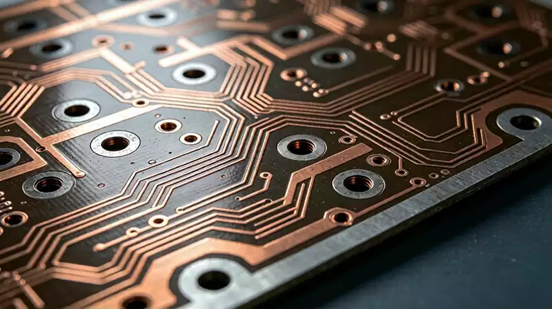
A bread board uses predetermined conductive groups and removable jumper wires. The engineer changes the circuit by physically moving components and wires. A PCB uses patterned copper traces, copper planes, pads, vias, and soldered components to create a fixed interconnection structure.
This difference becomes important when the design requires controlled electrical behavior. On a PCB, component placement and trace routing can be optimized to reduce unwanted loop area, improve grounding, shorten critical connections, and manage power distribution. A multilayer PCB can also incorporate dedicated power and ground planes, while high-speed designs can use controlled-impedance transmission lines and carefully defined return paths.
A PCB also provides a much more stable mechanical structure. Components are soldered to defined pads, connectors can be mechanically secured, and the finished board can be integrated into an enclosure. This makes the PCB suitable for repeatable testing, field use, and manufacturing.
The transition should therefore not be viewed simply as replacing one physical board with another. Moving from a bread board circuit to a PCB means converting an experimental physical arrangement into a controlled electrical and mechanical design.
When Should a Bread board Circuit Become a PCB?
The right time to move from a bread board circuit to a PCB depends on the development stage and the requirements of the application. If the circuit topology is still changing frequently, breadboarding remains useful because the cost of modification is low.
Once the circuit’s basic function has been validated and the component selection, power architecture, interfaces, and major electrical relationships have become stable, PCB design becomes more practical. The decision becomes even more important when the product needs a smaller form factor, reliable connectors, controlled signal paths, improved power integrity, thermal management, or repeatable assembly.
For example, a microcontroller project may begin with a development board and bread board circuit while firmware and sensor connections are being tested. After the interfaces and power requirements are confirmed, those functions can be incorporated into a custom PCB. The resulting board can place the microcontroller, power circuitry, connectors, sensors, and supporting components in fixed positions and route their connections according to the actual electrical requirements.
For high-speed digital, RF, precision analog, or switching power applications, the transition may need to happen earlier because the physical interconnect itself becomes part of the circuit behavior. A bread board can demonstrate basic functionality while still failing to reproduce the signal integrity, grounding, power distribution, or electromagnetic behavior that the final PCB must achieve.
From Bread board Circuit to PCB Prototype
A common mistake is to copy the physical bread board arrangement directly into a PCB layout. A breadboard is designed around convenience and flexibility, whereas a PCB should be designed around electrical performance, manufacturability, thermal behavior, mechanical requirements, and component placement.
The first step should therefore be to convert the working breadboard circuit into a clean schematic. Every component, power rail, signal connection, connector, and protection device should be represented explicitly. The schematic becomes the electrical reference for the PCB rather than the physical appearance of the breadboard.
The next stage is component and footprint selection. The actual package dimensions, pin assignments, thermal requirements, and availability of the selected components need to be confirmed before layout begins. This is especially important when moving from through-hole components used on a breadboard to surface-mount components used on a compact PCB.
PCB placement and routing can then be developed around the electrical priorities of the design. Decoupling capacitors should be positioned appropriately relative to the devices they support, high-current paths should use suitable copper geometry, sensitive analog signals should be separated from noisy switching nodes where necessary, and return-current paths should be considered together with the forward signal path.
After layout, a prototype PCB can be fabricated and assembled for validation. At this stage, testing should go beyond simply confirming that the circuit powers on. Power-rail stability, signal integrity, thermal behavior, connector fit, component temperatures, functional performance, and potential EMI issues should be evaluated according to the requirements of the application.
Why a Bread board Circuit Should Not Be Treated as the Final Design
A bread board circuit proves that a particular physical implementation can make the circuit operate under specific test conditions. It does not automatically prove that the circuit is ready for a PCB, let alone for production.
The PCB introduces a different physical environment. Trace impedance, copper resistance, parasitic capacitance, parasitic inductance, ground-plane structure, component placement, solder joints, thermal paths, and connector geometry all affect the final behavior. A circuit that works on a breadboard can therefore behave differently after being transferred to a PCB if the layout does not preserve the necessary electrical relationships.
This is why the bread board-to-PCB transition should include engineering review rather than simple redrawing. The goal is to preserve the intended circuit function while improving the physical implementation so that the design can operate reliably under its actual electrical, mechanical, and environmental conditions.
A bread board circuit remains one of the most practical methods for early electronic prototyping because it allows engineers to assemble and modify circuits without soldering. Its greatest strength is flexibility, which makes it particularly useful when the circuit is still being developed or when component values and connections need to be tested repeatedly.