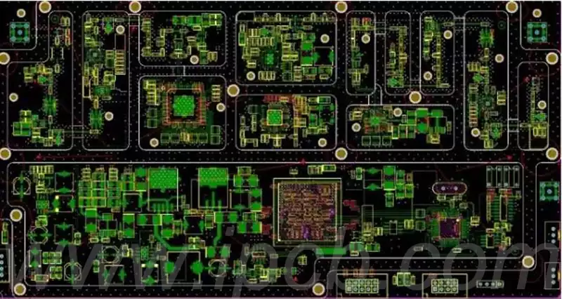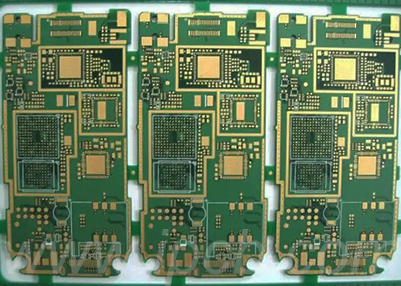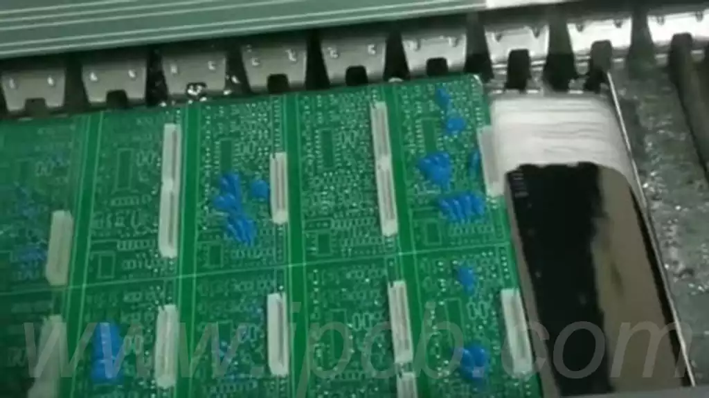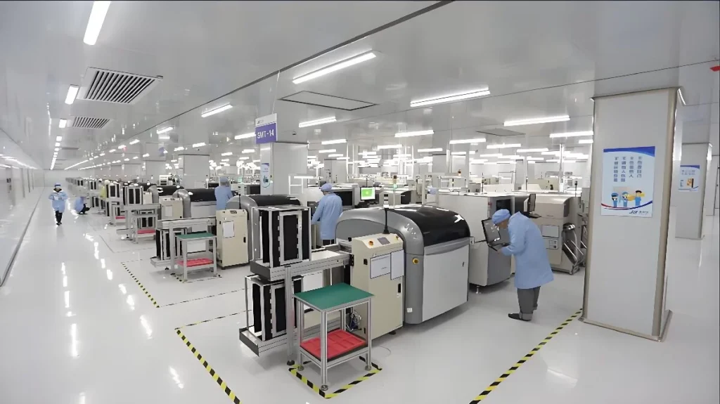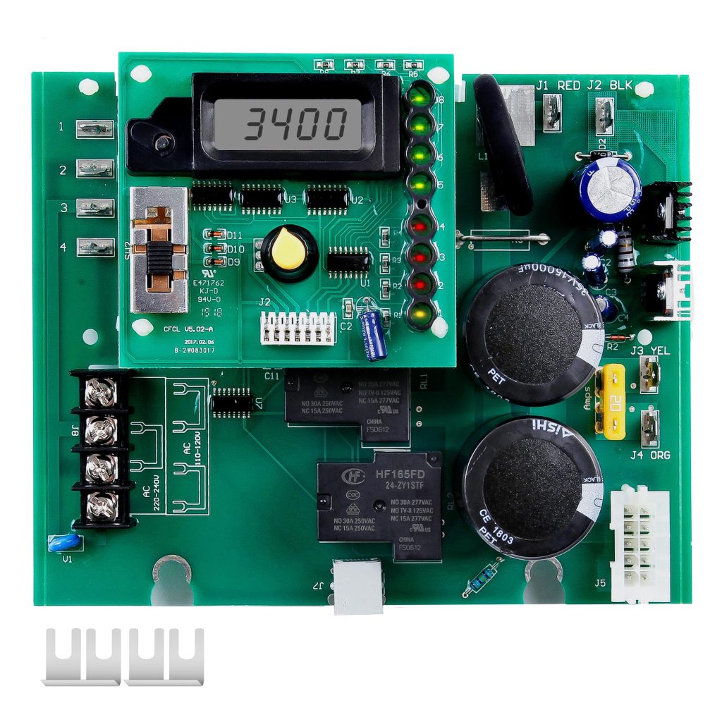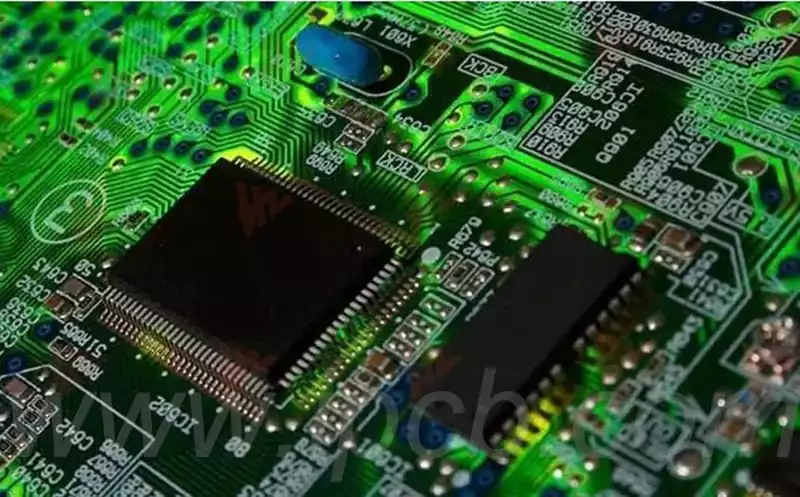
High speed pcb sheet in PCB manufacturing
High speed pcb sheet has the characteristics of low dielectric constant and low dielectric loss, which helps to significantly reduce the energy loss and distortion during the signal transmission process, thus improving the transmission speed and stability of the signal. In the high-frequency and high-speed digital signal transmission scenarios, the appropriate choice of high-speed sheet […]