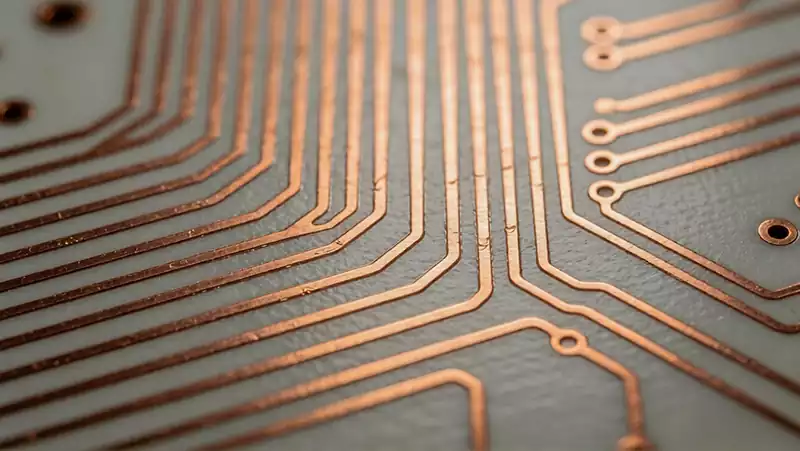
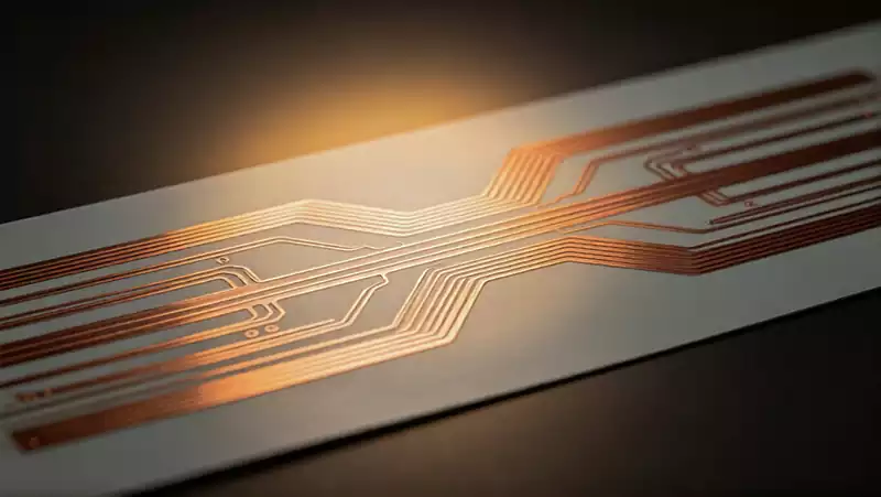
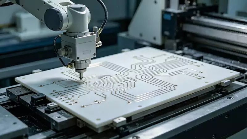
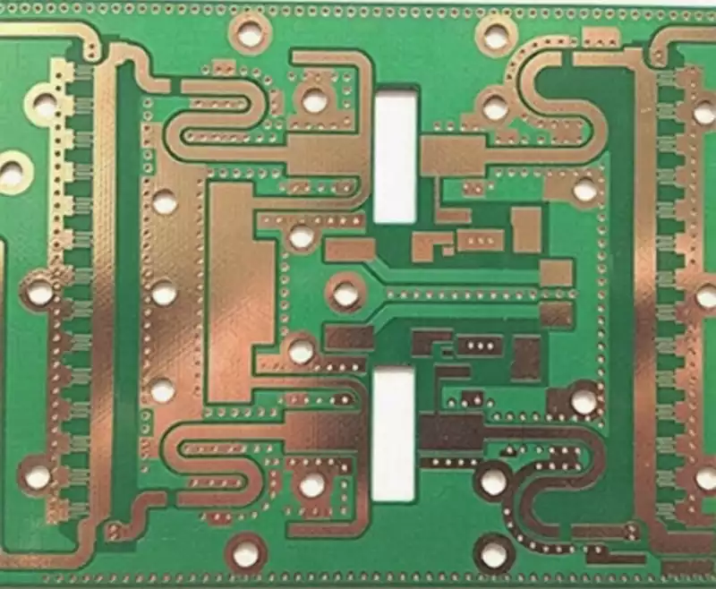
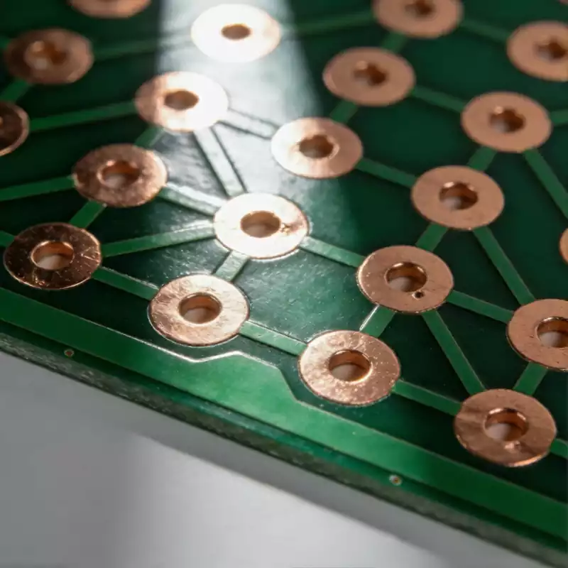
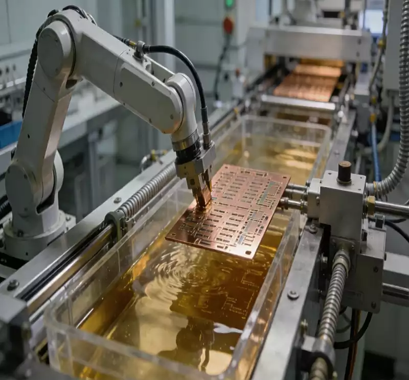
Technology Blog

ceramic circuit board

Thermal Conductivity Properties and Development Trends of Ceramic Circuit Boards

When the thermal conductivity of conventional FR-4 substrates, typically below 1 W/(m·K), proves inadequate for managing the thermal loads of high-power devices, ceramic circuit boards emerge as the preferred solution. Their exceptional thermal performance establishes them as a core component in high-end applications such as new energy vehicles, 5G communications, and medical equipment. As a […]

Analysis of high dielectric constant

In the wave of nanotechnology, two-dimensional materials have become a focus in the field of materials science due to their atomic scale thickness and unique physical properties. Among them, High-k 2D materials are gradually becoming a key force driving the innovation of electronic devices due to their excellent electrical properties and broad application prospects. Compared

pcb laminate

Key Considerations for PCB Laminate Design

In the field of electronic circuit design, the PCB (printed circuit board) serves as the substrate for electronic components, with its performance directly impacting the quality and reliability of the entire electronic product. PCB laminate design, as a critical component of PCB design, functions like the foundational structure of a precision-engineered building, playing a decisive

optical module pcb

Optical Module PCBs

As a core component in optical communications, the stability and reliability of optical modules are paramount. The optical modules pcb design not only determines their electrical performance but also plays a decisive role in thermal management, signal protection, and manufacturability. In the evolution of optical modules, PCBs predominantly adopt HDI structures—whether mechanical blind-via HDI, laser

Ceramic circuit boards

Ceramic circuit boards?

Ceramic circuit boards utilise ceramic as the substrate material, upon which metallic circuits are constructed and conductive vias formed. Ceramics encompass a diverse range of materials, with commonly employed types including aluminium oxide, aluminium nitride, zirconium oxide, silicon carbide, and silicon nitride – all classified as inorganic non-metallic materials. The fabrication of ceramic discs or

Drone PCB drives intelligent flight innovation

Drone PCB drives intelligent flight innovation

The Foundation of the Integration of Drones PCB Systems As highly integrated intelligent flight platforms, drone pcb have evolved from their original military reconnaissance tools to comprehensive systems widely used in a variety of fields, including aerial photography, logistics, agricultural monitoring, surveying and mapping, and even emergency rescue. Their complex flight control, navigation, image processing,

pcb circuit board

PCB Circuit Board Connection Methods

Connections between pcb circuit boards are primarily achieved through conductive connectors, wires, flexible printed circuits (FPC), board-to-board connectors, and soldering techniques. Among these, flexible printed circuits (FPC) serve as a widely adopted connection method, excelling in the creation of reliable, high-density electronic products. Their lightweight, thin profile and excellent flexibility make them highly suitable for

smt stenci

The Role and Classification of SMT Stencils in Surface Mount Technology

SMT stencils, commonly referred to as ‘templates’, are an indispensable component of the SMT (Surface Mount Technology) process; they serve as the template for printing solder paste onto the PCB (Printed Circuit Board) during the initial stage of surface mounting. In the first stage of the SMT process, this smt stencil is employed to precisely

PCB trace impedance

Factors Affecting PCB Trace Impedance and Calculation Methods

PCB trace impedance refers to the total resistance encountered by electrical signals during transmission across a PCB board. In layman’s terms, it represents the ‘resistance’ encountered by electrical signals as they traverse the PCB. PCB trace impedance matching denotes the adjustment and alignment of trace impedance to ensure more stable and reliable signal transmission across

semi flex pcb

Characteristics and Applications of Semi Flex PCB

Semi flex pcb is essentially “standard” multilayer PCBs manufactured using specific grades of FR4. The thickness of the FR4 is subject to particular tolerances, enabling thinner sections to provide the flexible/bendable portions traditionally achieved with rigid FR4. Semi flex pcb is suitable for static applications (where the flexible section aids assembly) or scenarios involving minimal

high speed pcb

Key Considerations and Strategies for High Speed PCB Design

High speed PCB design specifically refers to systems that utilise high speed digital signals to transmit data between components. The boundary between high-speed digital design and simpler circuit boards employing slower digital protocols is not always clear cut.Typically,the key indicator determining whether a system qualifies as ‘high-speed’ is the edge rate (or rise time) of

PCB impedance control

The Importance of PCB Impedance Control and Its Effects

The Impact of PCB Impedance Control on Circuit Performance and Stability. In the design of high-frequency, high-speed electronic products, the stability and reliability of circuit performance critically influence product quality. PCB impedance control, as one of the key factors affecting signal transmission quality, is an indispensable technique in high-quality circuit board design. PCB impedance control

flexible pcb

Methods for Enhancing the Reliability of Flexible PCB

Driven by innovation in consumer electronics, medical devices, aerospace, and other fields, flexible pcb (FPC) have become core components for achieving three-dimensional structural integration and dynamic functionality in devices. However, the physical properties of flexible substrates differ fundamentally from those of rigid PCBs. Relying solely on the inherent flexibility of the material cannot guarantee long-term

Rapid PCB Prototyping Applications in Electronics Development

Rapid PCB Prototyping Applications in Electronics Development

Introduction — What is Rapid PCB Prototyping? Rapid PCB prototyping (PCB) plays a crucial role throughout the entire electronics product development lifecycle. It’s a critical step in transforming design concepts from paper into verifiable prototypes, serving as a vital bridge from concept to finished product. Simply put, Rapid PCB Prototyping utilizes advanced manufacturing technologies and

silkscreen printing

PCB Silkscreen Printing Design

Silkscreen printing is typically employed to mark useful information on PCB boards, aiding users during the assembly process. It serves to label component values, part numbers, polarity, and other details, while also incorporating version numbers, manufacturer information, and similar data. PCB silkscreen printing is completed during the PCB manufacturing process, yet it is utilised in

Coverlay Flex PCB Applications and Future Trends

Coverlay Flex PCB Applications and Future Trends

Introduction and Background In modern electronic product design and manufacturing, flexible printed circuits (FPCs) have expanded from a limited number of high-end applications to encompass a wide range of fields, including consumer electronics, automotive electronics, medical devices, and aerospace. As products evolve toward thinner, lighter, more compact, and more reliable designs, FPCs are becoming more

rogers rt duroid

Rogers RT duroid high-frequency materials

Rogers RT duroid high-frequency circuit materials are composite laminates of PTFE (with random fillers of glass or ceramic), suitable for high-reliability applications such as aerospace. For many years, the RT/duroid series has been recognised within the industry as a high-reliability material offering exceptional performance. AdvantagesThe RT/duroid material series offers significant advantages including ultra-low loss, low

rigid pcb

The Difference Between Rigid PCB and Flexible PCB

Rigid PCB, commonly referred to simply as PCBs, are what most people envision when thinking of circuit boards. These boards utilise conductive tracks and other components arranged upon a non-conductive substrate to connect electrical components. In rigid circuit boards, the non-conductive substrate typically incorporates glass cloth, which enhances the board’s strength and imparts rigidity. Rigid

aluminium substrate

The Structure and Advantages of High-Conductivity Aluminium Substrate

Ultra-high thermal conductivity aluminium substrate is a novel circuit board that achieves exceptional thermal performance by replacing the resin insulating layer within existing metal aluminium-based circuit board structures with a multi-film layer nanostructure diamond-like carbon (DLC) insulating layer. Ultra-hyperconductive aluminium substrate is a utility model applicable to the printed circuit board field, providing an efficient

Millimetre Wave

What is 5G millimetre wave and Interconnect Design Optimisation Strategies

What is 5G millimetre wave? 5G millimetre wave, also known as the millimetre wave band, refers to the spectrum segment with wavelengths between 1mm and 10mm, corresponding to frequencies ranging from 30 to 300GHz. In practical applications, frequencies above 24GHz are classified as millimetre waves. This band occupies the overlapping wavelength range between microwaves and

pcb substrate

The Effects and Optimisation of Thermal Stress in PCB substrate

Thermal stress refers to the mechanical stress arising from uneven thermal expansion or contraction within materials during temperature changes. Within the PCB substrate sector, thermal stress primarily originates from the following sources: Thermal cycling during manufacturingReflow Soldering: In SMT processes, PCB substrate endure high temperatures (240–260°C) and rapid cooling. Non-uniform expansion and contraction of materials

rogers pcb

Rogers PCB Soldering Guide

Rogers PCB materials, owing to their unique properties, have become a critical choice in the manufacture of high-frequency electronic equipment. They find extensive application in wireless communication systems, satellite communication devices, radar systems, and microwave antennas. Their exceptional low loss, low dielectric constant, low dielectric loss factor, and outstanding dimensional stability enable Rogers PCBs to

Dry Film Solder Mask in PCB Manufacturing

Dry Film Solder Mask in PCB Manufacturing

Introduction and Background In the printed circuit board (PCB) manufacturing process, solder mask is a crucial step. It’s more than just a protective coating; it’s a key factor affecting soldering quality, circuit reliability, and overall circuit performance. The primary function of the solder mask is to cover the copper foil surface, protecting the circuit from

glass substrate

Technologies and Prospects for Glass Substrates in Chip Packaging

Chip packaging technology constitutes a critical component within the semiconductor industry, directly influencing the performance, reliability, and lifespan of electronic devices. In recent years, as electronic products have evolved towards miniaturisation and enhanced performance, traditional packaging materials have progressively revealed their limitations. Against this backdrop, glass substrates, owing to their unique physicochemical advantages, are increasingly

Scroll to Top