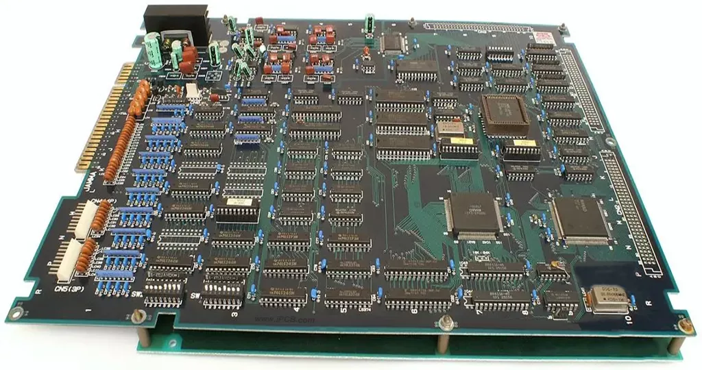
The PCB pad, as a critical part connecting components to the PCB, directly determines the performance and stability of the entire circuit. However, in actual production and maintenance processes, pad detachment issues occur from time to time. This not only leads to circuit failures, affecting the normal use of products, but also increases maintenance costs and time. A thorough analysis of the causes of pad detachment and a grasp of scientific and effective repair process points are crucial for ensuring the quality and reliability of electronic products.
Causes of PCB Pad Detachment
Improper Maintenance Operations
Improper heating control is the primary cause. During maintenance, errors in controlling the temperature and heating time of tools such as hot air guns and soldering irons can directly damage the bonding force between the pad and the PCB substrate. For example, setting the hot air gun temperature above 280°C (with conventional pad tolerance temperatures ranging from 240-260°C) or heating a single point for more than 10 seconds can cause carbonization and failure of the adhesive at the bottom of the pad, leading to peeling and detachment. Some operators, in pursuit of faster disassembly speeds, use high temperatures to bake the pad area for extended periods, which not only damages the pad but also causes yellowing and delamination of the PCB substrate, exacerbating failures.
Improper tool usage and operating techniques can also cause problems. Using a pointed soldering iron and pressing or prying on the pad or component leads with force can directly tear the pcb pad. When disassembling through-hole components, forcibly inserting or removing without first melting the solder can transmit external force through the leads, causing pad detachment. Additionally, excessive solder during welding or poor-quality solder paste can generate excessive thermal stress during heating, indirectly damaging the connection between the pad and the substrate.
Non-standard maintenance procedures can also pose hidden dangers. For example, failing to clean the pad area before disassembling components can leave residues of flux, dust, and other contaminants that affect heating uniformity, leading to localized overheating. Failing to cool sufficiently after repair and immediately moving or touching the pad area can cause stress from thermal expansion and contraction, leading to secondary pad detachment.
Quality Issues with PCB Substrates
The quality of the PCB substrate directly determines the adhesion strength of the pcb pad. Poor-quality substrates or those with inherent defects can lead to pad detachment even with proper maintenance operations. For example, if the copper foil thickness of the copper-clad laminate used in the substrate is insufficient (below 1oz) or if the bonding force between the copper foil and the epoxy resin substrate is poor, the pad can easily peel or detach under minor external force or thermal stress. In some low-cost PCBs, the pad surface is not subjected to anti-oxidation treatment (such as immersion gold or tin plating), or the treatment process is substandard, making the pad prone to oxidation and corrosion. Heating during maintenance can accelerate the detachment of the oxide layer, damaging the pad along with it.
Additionally, unreasonable PCB design can also increase the risk of pad detachment. For example, if the pad size is too small and poorly compatible with the component leads, stress is concentrated during welding. If the connection between the pad and the wire is too narrow, forming a “stress concentration point,” thermal stress and external force during maintenance can easily cause breakage at that point, leading to pad detachment.
Indirect Effects of Environmental and Storage Factors
The storage and usage environments of PCBs can indirectly reduce the adhesion strength of pads, increasing the probability of detachment during maintenance. Long-term storage in high-temperature, high-humidity environments can cause the PCB substrate to absorb moisture, leading to hydrolysis and aging of the adhesive at the bottom of the pad, reducing the bonding force between the pad and the substrate. If the storage environment contains acidic or alkaline gases, dust, or other contaminants, they can corrode the pad surface and substrate, exacerbating the risk of pad detachment.
For PCBs already in use, prolonged exposure to vibrations and alternating high and low temperatures (such as in automotive or industrial control equipment) can cause the pad to repeatedly withstand stress from thermal expansion and contraction and mechanical vibrations, gradually loosening the connection between the pad and the substrate. Slight heating or touching during maintenance can then cause detachment.
External Force Damage from Improper Component Disassembly
One of the core aspects of PCB maintenance is component disassembly. If the disassembly method is improper, external force can be transmitted through the component leads, directly causing pad detachment. For example, when disassembling dense-pin components such as QFPs and BGAs, failing to use dedicated disassembly tools or failing to uniformly heat all leads can result in some leads melting the solder while others remain solid. Forcibly prying the component can then pull on the pads. When disassembling through-hole components, using pliers or other tools to directly clamp and forcibly insert or remove the leads can apply external force directly to the pads, causing them to tear and detach.
Key Process Points for PCB Pad Repair
Selection of Tools and Materials: Adaptability is the Core
The selection of repair tools and materials should align with the pad size, PCB substrate type, and repair level to prevent secondary damage caused by inappropriate tools or materials. The key selection points are as follows:
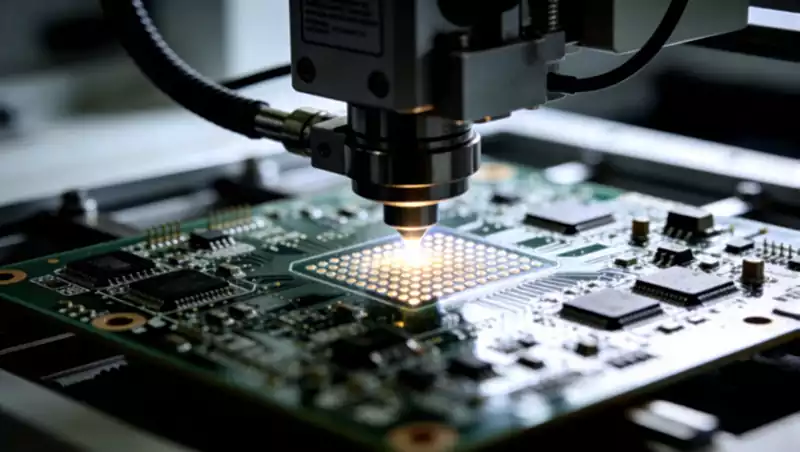
Heating Tools: Prioritize the use of constant-temperature hot air guns and antistatic soldering irons. The hot air gun should support precise temperature adjustment (with an error not exceeding ±10°C) and be equipped with nozzles of different sizes to accommodate pads of varying sizes. The soldering iron should have a pointed or angled tip with a power rating between 20-30W to avoid excessive local heating due to high power. For pads corresponding to dense-pin components, a miniature hot air gun is recommended to ensure uniform heating without damaging surrounding components.
Soldering Materials: Choose low-temperature solder paste (with a melting point of 138-150°C) to prevent excessive thermal stress during heating that could damage the substrate and pad. Select lead-free, no-clean flux to minimize residue and avoid corrosion of the pad and substrate. For repairing level-three damage, use high-viscosity, high-temperature-resistant epoxy resin adhesive to ensure reliable substrate repair and pad reinforcement. For cleaning materials, use anhydrous ethanol or specialized PCB cleaners, avoiding strongly corrosive cleaners that could damage the substrate and components.
Auxiliary Tools: Prepare a magnifying glass (10-20x) or microscope for observing pad details and repair results. Have antistatic tweezers, fine sandpaper (800-1000 grit), and fine copper wire (diameter 0.1-0.2mm) on hand for pad positioning, oxide layer polishing, and wire connections. Prepare a constant-temperature oven for curing epoxy resin adhesive and post-repair drying.
Cleaning and Pre-treatment
Cleaning and pre-treatment are fundamental steps in pad repair. Inadequate cleaning can lead to poor solder wetting, weak pad adhesion, and subsequent secondary detachment. The key operational specifications are as follows:
Cleaning Scope: Clean not only the area where the pcb pad has detached but also the surrounding 1-2mm area to remove flux residues, dust, oil, oxides, and other contaminants, ensuring the repair area is free of impurities.
Cleaning Methods: Use a cotton swab dipped in anhydrous ethanol or a specialized PCB cleaner to gently wipe the repair area, repeating the process 2-3 times until the cotton swab shows no stains. For stubborn flux residues, lightly heat with a soldering iron to melt the residue before wiping. For oxide layers, gently polish with fine sandpaper, applying light pressure to avoid damaging the PCB substrate and surrounding traces. Immediately wipe clean with a cleaner after polishing to prevent re-oxidation.
Pre-treatment: After cleaning, place the PCB in a constant-temperature oven at 60-80°C for 10-15 minutes to remove moisture from the PCB substrate and pad, preventing bubble formation due to water vaporization during heating repair, which could affect pad adhesion. For detached pads with oxide layers on their surfaces, perform the same polishing, cleaning, and drying procedures.
Heating Temperature and Time
Heating temperature and time are critical control points in pad repair and are key to avoiding secondary pad damage and substrate delamination. The heating parameters vary depending on the repair level and pad size. The key specifications are as follows:
Temperature Control: For conventional pad repair, set the hot air gun temperature between 240-260°C and the soldering iron temperature between 230-250°C. For small pads (size < 1mm), reduce the temperature to 230-240°C to prevent burning the pad and substrate. For level-three substrate repairs, the temperature can be set between 250-260°C, but the heating time should be shortened to avoid substrate delamination.
Time Control: Limit single heating sessions to no more than 10 seconds. If the desired adhesion is not achieved after one heating, allow a 3-5 second cooldown before reheating. Repeat the heating process no more than three times. For minor detachment (level-one damage), heat for 3-5 seconds; for moderate detachment (level-two damage), heat for 5-8 seconds; and for severe detachment (level-three damage), heat for 8-10 seconds. During heating, move the hot air gun evenly to avoid prolonged single-point heating, ensuring uniform solder melting and thorough pad-substrate adhesion.
Precautions: During heating, avoid sensitive components nearby (such as capacitors, resistors, and IC chips). Cover them with high-temperature-resistant tape beforehand to prevent damage from high temperatures. If the substrate turns yellow or smokes during heating, immediately stop heating, allow it to cool, assess the damage level, and adjust the repair plan.
Soldering and Fixing
The soldering and fixing process must ensure precise pad positioning and firm adhesion to avoid issues such as cold solder joints, false solder joints, and pad misalignment. The key operational specifications are as follows:
Pad Positioning: Align the detached pad or a new pad precisely with the pad imprint or corresponding position on the substrate. Gently press it in place with antistatic tweezers to ensure alignment between the pad and trace connection points without misalignment. For small pads, use a magnifying glass to assist with positioning for accuracy.
Solder Paste Application: Apply an appropriate amount of solder paste to avoid excessive amounts that could cause solder flow and short circuits or insufficient amounts that could result in weak adhesion. Evenly apply the solder paste to the bottom, surrounding areas, and trace connection points of the pad to ensure full coverage of the adhesion surface.
Soldering Operation: Use a hot air gun to evenly heat the pad area. After the solder paste has completely melted, gently release the tweezers and continue heating for 1-2 seconds to ensure firm adhesion between the pad, substrate, and trace. Immediately stop heating after completion and allow the PCB to cool naturally to room temperature. Do not touch the pad area with your hands to prevent stress from thermal expansion and contraction, which could cause secondary pad detachment.
Reinforcement Treatment: For level-two and level-three repairs, apply a small amount of epoxy resin adhesive around the pad after cooling to cover the joint between the pad edge and substrate, enhancing the pad’s mechanical strength. Apply the adhesive in an appropriate amount to prevent it from flowing onto the pad surface and affecting subsequent component soldering. After application, place the PCB in a constant-temperature oven at 80-100°C for 20-30 minutes to fully cure the adhesive.
Post-Repair Inspection
Post-repair inspection is the final line of defense to ensure pad reliability. A comprehensive inspection must be conducted to confirm the absence of hidden issues before the PCB can be put into use. The key inspection items and specifications are as follows:
Visual Inspection: Use a magnifying glass (10-20x) to observe the pad repair area, confirming precise pad positioning without misalignment, lifting, bubbles, or cold solder joints. The pad should be firmly connected to the substrate and trace without fractures or looseness. The surrounding substrate should show no yellowing, delamination, or damage. The epoxy resin adhesive should be evenly cured without flowing or residue.
Electrical Performance Inspection: Use a multimeter to test the conductivity between the pad and corresponding trace or component lead, confirming the absence of short circuits, open circuits, or cold solder joints. For high-end PCBs, perform insulation testing and signal transmission testing to ensure the repaired pad does not affect the PCB’s electrical performance or signal integrity.
Mechanical Strength Testing: Gently press the pcb pad with antistatic tweezers to test its firmness. It is considered qualified if there is no looseness or detachment. For PCBs with high-strength requirements, such as those used in automotive or industrial control applications, perform pull testing to ensure the pad’s pull strength is not less than 80% of the original pad’s strength.
Temperature Resistance Testing: Place the repaired PCB pad in a constant-temperature oven at 120-150°C for 1 hour. After cooling, perform visual and electrical performance inspections again to confirm the absence of pad detachment or abnormalities, ensuring it can withstand temperature changes in subsequent use environments.
The issue of PCB pad detachment involves various aspects such as maintenance operations, substrate quality, environmental storage, and component disassembly. Only by comprehensively understanding these causes can targeted measures be taken during the repair process to ensure the reliability and stability of the PCB, providing a solid guarantee for the normal operation of electronic products.