In the grand narrative of the booming development of modern electronics and information technology, whether it’s artificial intelligence computing clusters, 5G and future communication base stations, new energy vehicle electronic control systems, or precision medical instruments and aerospace payloads, the physical realization of all electronic functions relies on a seemingly thin yet intricately complex printed circuit board (PCB). If semiconductor chips are the “brain” that gives devices logic and computing power, then PCBs are the “neural network and vascular skeleton” that runs through the entire system. The industrial force that transforms these precise micron-level conductive patterns, insulating media, and interlayer interconnects from blueprints into reality is the global network of pcb circuit board manufacturers.
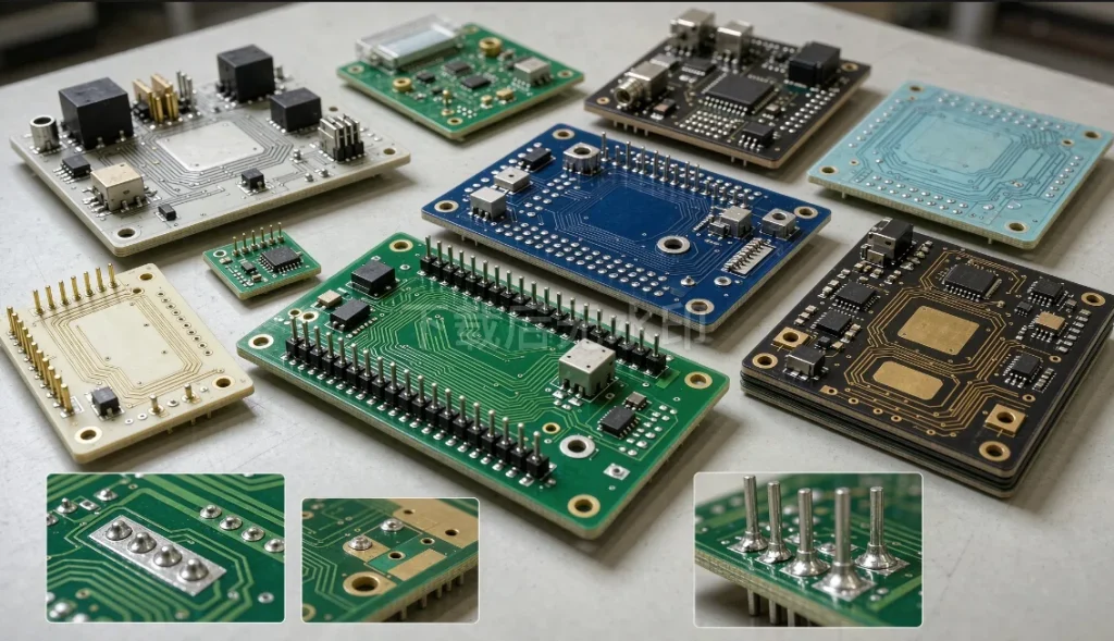
As end-user electronic products evolve towards high frequency, high speed, high-density interconnects, miniaturization, and high reliability, PCB manufacturing has long since moved beyond the early, simple workshop model of “copper-clad laminate etching and drilling,” evolving into a systems engineering discipline integrating polymer chemistry, electromagnetic field theory, precision machining, electrochemical deposition, optical lithography, and automated testing. Manufacturers of different sizes and technological focuses play drastically different roles in the industry chain: Ultra-large giants dominate the super-production lines for consumer electronics and packaging substrates with their staggering capital expenditures and production capacity, while specialized manufacturers with agile engineering response and capabilities in multiple high-difficulty processes become key drivers in R&D prototyping, high-frequency microwave, rigid-flex bonding, and one-stop assembly.
Global PCB Industry Landscape and Ultra-Large Manufacturers Overview
Looking at the global printed circuit board (PCB) industry landscape, East Asia has long held a core hub position in manufacturing and supply chains, encompassing major industrial clusters such as mainland China, Taiwan, Japan, and South Korea. Meanwhile, North America and Europe maintain significant R&D and manufacturing capabilities in aerospace, defense, automotive electronics, and specialized high-frequency fields. Within this vast PCB manufacturer ecosystem, ultra-large manufacturers typically possess extremely high annual revenue, multiple modern production bases, and strong vertical integration capabilities, enabling them to handle millions or even tens of millions of orders from leading global technology brands.
In industry observations and global rankings, Zhen Ding Technology Group has consistently ranked among the top global printed circuit board (PCB) manufacturers in terms of revenue, possessing massive production capacity in flexible printed circuit boards (FPCBs), high-density interconnect boards, and consumer electronics and communication boards. Unimicron, on the other hand, has deep expertise in high-end high-density interconnect boards and integrated circuit packaging substrates. With the increasing demand for advanced packaging substrates from artificial intelligence and high-performance computing, its technology and production capacity layout are attracting significant attention. Nippon Mektron enjoys a strong reputation in the flexible printed circuit board field, deeply serving mobile terminals, automobiles, and precision instruments with its precise roll-to-roll and highly reliable flexible manufacturing processes. Furthermore, TTM Technologies demonstrates strong engineering capabilities in high-density interconnects, RF microwaves, and defense, aerospace, and automotive electronics; Shennan Circuits has built a complete technology system in communication equipment backplanes, high-speed multilayer boards, high-density interconnects, and packaging substrates; and Japanese companies such as Ibiden are also among the world’s leading companies in high-end packaging substrates and cutting-edge microelectronic interconnect materials. The core competitiveness of these large manufacturers lies in their “extreme economies of scale” and “deep integration with leading customers.”
However, in actual R&D and small-batch delivery scenarios, many R&D teams, industrial equipment manufacturers, and innovative enterprises often face real pain points such as tight deadlines, diverse board types, special materials, and frequent design iterations. At this time, professional manufacturers that can provide rapid engineering response, flexible multi-process coverage, and one-stop delivery from bare board to assembly demonstrate unique and irreplaceable value.
Focus on iPCB: Agile Engineering and Manufacturing Practices Across the Entire Process Chain
Among numerous professional manufacturing service providers, iPCB is positioned as “reliable, fast, and professional,” deeply cultivating printed circuit board (PCB) design, prototyping, small-batch and large-batch manufacturing and assembly services. It has accumulated rich engineering experience in fields such as communication networks, industrial control, medical equipment, aerospace, semiconductor test boards, servers, automotive electronics, and microwave RF.
According to its publicly available information on process capabilities and service systems, iPCB not only possesses full-process manufacturing and testing equipment but also has established a rapid-response engineering support mechanism. It can provide design-to-manufacturer (DFM) feedback before quoting, helping customers identify potential issues with linewidth and spacing, impedance matching, aperture ratio, or stack-up structure before production, thereby shortening the R&D cycle and reducing trial-and-error costs. For hardware engineers, this model, where the engineering team directly intervenes in drawing review and process communication, often ensures a higher first-time success rate for complex boards than simply relying on automated quotation systems.
In terms of manufacturing collaboration and delivery models, iPCB balances prototyping agility with batch stability, supporting the transition from small-batch verification in the R&D prototype stage to stable mass production in the mature stage. Whether it’s a standard double-sided board, a high-layer rigid board, or a high-end board involving special dielectric materials and complex interlayer interconnections, its manufacturing and quality control systems revolve around on-time delivery, traceability, and process consistency.
High-end board process matrix: High-layer, HDI, rigid-flex, and high-frequency microwave.
The key to measuring a PCB circuit board manufacturer’s core technological strength lies in its ability to handle complex process matrices beyond conventional double-sided boards. Modern high-end electronic systems place almost stringent demands on space utilization, signal transmission rates, and structural adaptability, driving manufacturing processes to extend in multiple dimensions.
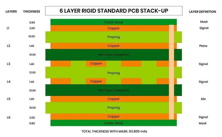
High-multilayer boards and precision pattern transfer: With the surge in pin counts for servers, network switches, and high-end test instruments, the number of circuit board layers continues to climb. High-multilayer board manufacturing not only requires extremely high interlayer alignment accuracy to prevent drilling from deviating from inner layer pads, but also presents stringent challenges to resin flow and filling, board thickness uniformity, and thermal expansion matching during the lamination process. In the pattern transfer stage, using Laser Direct Imaging (LDI) instead of traditional film exposure enables higher precision and consistency in finer linewidth and spacing, as well as solder mask window control.
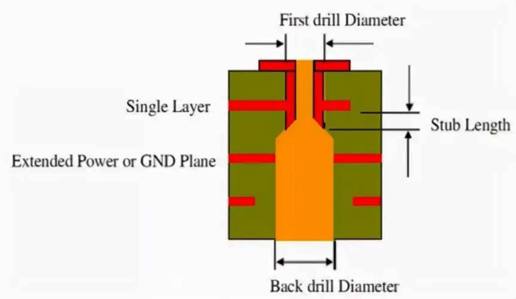
High-Density Interconnect (HDI) and Blind/Buried Via Technology: As component packages become smaller and pin pitches become denser, traditional mechanical through-holes occupy a significant amount of valuable wiring space. High-Density Interconnect (HDI) technology uses laser drilling to create micro-blind vias, combined with buried vias and arbitrary-layer interconnects or multi-level HDI structures, significantly increasing wiring density per unit area while shortening signal interconnect paths, thus improving the transmission quality of high-speed signals. The quality of desmearing and electroplating filling after laser drilling directly determines the long-term reliability of the microvias under thermal shock.
Rigid-Flex PCBs: Three-Dimensional Spatial Adaptability. In foldable terminals, medical wearables, precision camera modules, and compact automotive spaces, rigid-flex PCBs integrate the robust component support of rigid boards with the dynamic bending capabilities of flexible boards. The manufacturing challenge lies in the differences in lamination temperature, material thermal expansion coefficient, and bending stress between the rigid and flexible regions. Improper design of the bending area or lamination process control can easily lead to copper foil fatigue cracking or delamination due to repeated bending. Therefore, precise coordination is required in material selection, adhesive matching, and bending area structure planning.
In high-frequency microwave boards and mixed-lamination processes, high-frequency signals are common in RF communication, millimeter-wave radar, and microwave front-end applications. The dielectric loss and dielectric constant stability of traditional epoxy resin fiberglass cloth substrates often fail to meet requirements. Manufacturers with high-frequency capabilities, such as iPCB, typically stock a variety of high-frequency, high-speed materials, including Rogers, PTFE, hydrocarbons, and Panasonic Megtron, and support multi-material mixed lamination of high-frequency materials with conventional FR-4. Mixed-lamination manufacturing requires precise control of the flow and adhesion states of different dielectric materials under lamination temperature and pressure curves, while also considering the impact of copper foil surface roughness on high-frequency skin effect losses.
Materials Science and Supply Chain Assurance: Substrate Selection and Process Window
In printed circuit board (PCB) manufacturing, “even a skilled cook cannot make a meal without rice.” No matter how advanced the etching, drilling, and electroplating equipment, without a stable and reliable raw material system, it is impossible to produce highly reliable PCBs. High-quality PCB manufacturers often establish multi-brand, multi-specification substrate libraries, covering epoxy resin materials with different glass transition temperature (Tg) levels, halogen-free environmentally friendly substrates, high thermal conductivity metal-based materials, and various high-frequency, high-speed boards. In engineering practice, materials with higher Tg can better maintain dimensional stability and suppress vertical expansion stress during high-temperature reflow soldering or long-term high-temperature operation, thereby reducing the risk of via breakage; while halogen-free materials comply with the requirements of green environmental regulations for flame-retardant systems. Besides the materials themselves, the stability of the supply chain and batch traceability are equally crucial. In industries such as communications, industrial, and medical, the batch management of components and substrates directly affects the lifespan of the entire device and the risk of recall. Reliable manufacturers maintain complete batch and process records at key stages such as raw material warehousing, cutting, lamination, surface treatment, and testing. They also proactively inform customers of risks when the laminated structure exceeds the standard process window, avoiding potential quality issues later on due to blindly accepting orders.
From Bare Board to PCBA One-Stop Delivery: Seamless Integration of Manufacturing and Assembly
For many electronics companies, separately seeking bare board manufacturers, component sourcing channels, and surface mount assembly plants not only incurs high communication costs but also easily leads to blame-shifting in case of soldering defects or electrical failures. Therefore, manufacturers that can provide one-stop services for printed circuit board manufacturing and printed circuit board assembly (PCBA) are increasingly favored by the market. Moving from bare boards to assembled finished products represents a leap from “geometric manufacturing” to “microscopic metallurgy and thermodynamic bonding.” In surface mount technology (SMT) and through-hole mounting (THT) processes, the surface treatment of pads (such as HASL solder mask, ENIG immersion gold, and OSP organic solderability protectant), the rationality of pad design and solder mask openings, the matching of stencil openings, and whether the reflow soldering temperature profile has been adequately thermally profiled all directly affect the wettability, intermetallic compound formation, and mechanical strength of the solder joints. When bare board manufacturing and assembly processes are carried out collaboratively within the same system, DFM (Design for Manufacturing) reviews can cover the entire chain from pad geometry to component package spacing, and from thermal pads to test point layout. Teams like iPCB, which cover PCB manufacturing and PCBA assembly, testing, and related services, can integrate assembly process requirements into board manufacturing and engineering preparation early on, reducing information loss during cross-factory coordination and accelerating the overall pace from prototype verification to mass production delivery.
Quality Control and Testing Verification: IPC Standards, AOI (Automated Optical Inspection), and Electrical Testing
In today’s world, where micron-level linewidths and high-density interconnects are the norm, visual inspection alone is no longer sufficient to maintain quality standards. Professional manufacturing systems typically use internationally recognized IPC standards (such as IPC-A-600 for appearance and acceptance, and Class 2 or Class 3 for higher reliability requirements) and quality management systems (such as ISO 9001 and IATF 16949) as benchmarks to build multiple lines of defense for inspection. In the process and shipment verification stages, automated optical inspection (AOI) can quickly compare graphics and design data to identify defects such as open circuits, short circuits, residual copper, gaps, and solder mask misalignment; electrical continuity and insulation testing (such as flying probe testing or dedicated E-test fixtures) verifies network connectivity one by one, preventing hidden open circuits or micro-short circuits from flowing downstream; for high-requirement orders, cross-section analysis can also be used to check whether the copper thickness of vias, lamination voids, and dielectric layer thickness meet specifications. These interconnected physical and electrical verification methods constitute the final safety gate for the long-term stable operation of electronic products.
Conclusion: Moving towards the future through precision manufacturing and agile collaboration
Looking back at the entire electronics manufacturing industry chain, PCB circuit board manufacturers are not only the physical implementers of cutting-edge hardware innovation, but also masters of balancing industrial reliability and cost control. Whether it’s the massive consumer electronics boom supported by ultra-large manufacturers with huge production capacity, or powerful manufacturers like iPCB that empower R&D and manufacturing with multi-process coverage, high-frequency special materials reserves, rapid engineering response, and one-stop PCB/PCBA services, they are all driving electronic hardware towards higher performance and higher reliability in their respective tracks. For electronic engineers and purchasing decision-makers, understanding the technological boundaries, material systems, and quality control logic of different manufacturers is far more important than simply comparing price lists. Only by deeply integrating precise design intent with solid manufacturing processes can each circuit board operate steadily in the real physical world, carrying the infinite possibilities of the next generation of smart technologies.