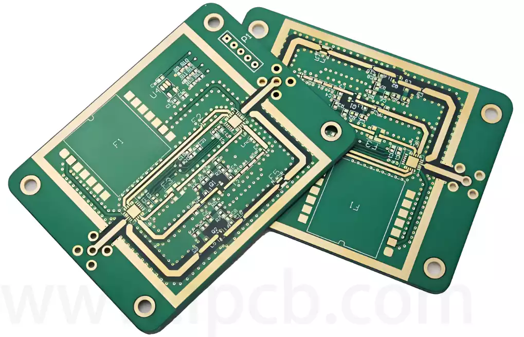
A custom PCB circuit board is developed around the electrical, mechanical, and environmental requirements of a specific electronic product. Unlike standard circuit boards designed for general applications, a custom PCB allows engineers to define the board dimensions, layer structure, material, copper thickness, and circuit layout according to the intended design. This flexibility makes custom PCBs suitable for products with specialized functions, limited installation space, particular electrical requirements, or production constraints.
However, customizing a circuit board involves more than changing its shape or adding circuit layers. Material properties, trace geometry, component placement, thermal performance, and manufacturing capabilities all influence whether a design can be produced reliably. Understanding these factors before production helps engineers avoid unnecessary revisions and ensures that the finished board meets the requirements of its application.
What Is a Custom PCB Circuit Board?
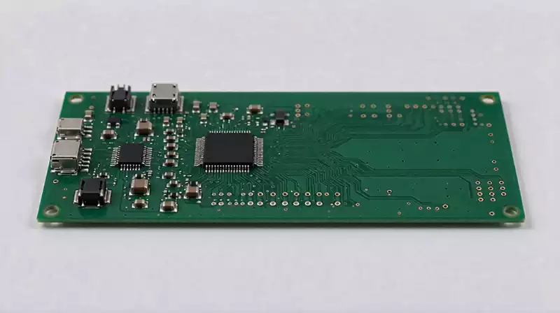
A custom PCB circuit board is a printed circuit board manufactured according to customer-specific design files and technical specifications. It provides the conductive paths and mechanical support needed to connect electronic components, while its structure is adapted to the requirements of the final product.
Depending on the application, a custom PCB may be single-sided, double-sided, or multilayer. It can also use different substrate materials, copper weights, board thicknesses, surface finishes, and via structures. For example, a simple control circuit may only require a two-layer FR-4 board, while a high-speed communication device may need a multilayer stack-up with controlled impedance and carefully arranged reference planes.
Custom PCBs are used in industrial equipment, consumer electronics, automotive systems, medical devices, communication products, power electronics, and many other applications. Their specifications vary because each product has different requirements for electrical performance, physical dimensions, operating conditions, and manufacturing cost.
Why Choose Custom PCB Manufacturing
Custom PCB manufacturing gives engineers greater control over the circuit board’s construction and performance. When a product has a specific enclosure size, connector position, or mounting arrangement, a custom board can be designed to fit the available space without relying on a standard board format. This is particularly useful for compact electronic devices and equipment with unusual mechanical layouts.
Electrical requirements are another reason to choose a custom PCB. Engineers can arrange signal, power, and ground layers according to the circuit’s needs, adjust trace widths for current capacity, and specify controlled impedance where necessary. These design choices help the board support the intended operating conditions instead of forcing the circuit to adapt to the limitations of a standard product.
Customization also allows manufacturers to select materials and production processes that match the application. A high-temperature industrial controller, for example, may require a different laminate from a low-cost consumer device. Similarly, a high-current power board may need heavier copper and a layout that provides adequate heat distribution. The goal is to specify only the features that the application actually requires, balancing performance, manufacturability, and cost.
Types of Custom PCB Circuit Boards
The appropriate PCB structure depends on circuit complexity, available space, electrical requirements, and production volume. Single-sided PCBs have conductive copper on one side of the substrate and are generally used for relatively simple circuits. Their straightforward construction can make them a cost-effective option when routing density and electrical requirements are limited.
Double-sided PCBs use copper layers on both sides of the substrate, with plated through-holes connecting the two sides where required. This structure provides more routing flexibility than a single-sided board and is suitable for many control circuits, power supplies, and electronic products.
Multilayer PCBs contain three or more conductive layers laminated together with insulating materials. They provide greater routing density and allow engineers to allocate dedicated layers for signals, power, and ground. Multilayer construction is commonly used in communication equipment, industrial controllers, computers, and other products with complex circuit requirements.
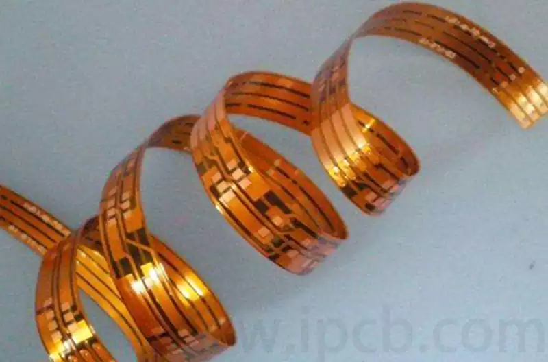
Rigid, flexible, and rigid-flex PCBs offer different mechanical characteristics. Rigid boards maintain a fixed shape and are widely used in conventional electronic assemblies. Flexible PCBs use bendable substrates for applications where circuits must fit into curved or moving structures. Rigid-flex boards combine rigid sections with flexible interconnections, making them useful when both mechanical stability and space-saving routing are needed.
Material Selection for Custom PCB Circuit Boards
The substrate material affects a PCB’s electrical insulation, thermal behavior, mechanical strength, and manufacturing characteristics. FR-4 is widely used because it offers a practical balance of performance, availability, and cost. It is suitable for many consumer electronics, industrial control boards, and general-purpose electronic assemblies.
When the application involves higher operating temperatures or more demanding assembly conditions, high-Tg FR-4 may be considered. Its glass transition temperature is higher than that of standard FR-4, which can provide better dimensional stability under elevated temperatures. However, Tg alone does not determine whether a material is suitable for an application. Engineers should also consider decomposition temperature, coefficient of thermal expansion, thermal conductivity, and the expected operating environment.
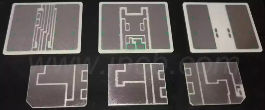
High-frequency applications may require specialized laminates with controlled dielectric properties and low signal loss. Materials based on PTFE or hydrocarbon ceramic systems are used in certain RF, microwave, and high-speed communication designs. Aluminum-based PCBs are another option for applications that need a particular thermal construction, such as some LED and power-related products. The final material should be selected according to the complete electrical, thermal, and mechanical requirements rather than a single specification.
PCB Layer Stack-Up and Design Considerations
The layer stack-up defines how copper and dielectric layers are arranged within the PCB. A suitable stack-up supports routing requirements while helping control impedance, signal integrity, electromagnetic interference, and board warpage. In multilayer designs, engineers should consider the position of signal layers relative to their reference planes, dielectric thickness, copper distribution, and the routing needs of power and ground networks.
Board thickness is another important specification because it affects mechanical strength, component clearance, connector compatibility, and the overall dimensions of the finished product. Common thicknesses may be suitable for many standard applications, but the final value should be based on enclosure requirements, mounting conditions, and the manufacturer’s available materials and processes.
Trace width and spacing must also be defined according to current capacity, voltage clearance, signal requirements, and fabrication tolerances. High-current circuits may require wider traces or heavier copper, while dense designs may need finer line widths and spacing. Engineers should confirm that these features are within the manufacturer’s capabilities before releasing the design for production.
Via design is equally important in multilayer PCBs. Through-hole vias connect different layers across the board, while blind and buried vias can provide additional routing flexibility in more complex designs. These structures may increase manufacturing complexity and cost, so they should be used only when the electrical or space requirements justify them.
Surface Finishes for Custom PCB Manufacturing
The surface finish protects exposed copper and provides a solderable surface for component assembly. Different finishes offer different characteristics, and the appropriate choice depends on the assembly process, component types, storage conditions, and budget.
HASL is a widely used finish that provides good solderability and is available in leaded and lead-free versions. However, its relatively uneven surface may make it less suitable for some fine-pitch components. ENIG provides a flatter surface and is commonly selected for fine-pitch assembly and applications requiring good surface protection, although its cost is generally higher than that of HASL.
OSP is an organic coating applied to exposed copper and is often used when cost and a flat surface are important. Immersion silver is another option for certain designs, although handling and storage conditions need to be considered. No surface finish is ideal for every PCB. The selection should match the component footprint, soldering requirements, expected storage period, and final product specifications.
The Custom PCB Circuit Board Manufacturing Process
Custom PCB manufacturing begins with an engineering review of the customer’s design data. The manufacturer checks the Gerber files, drill files, stack-up, board dimensions, copper requirements, surface finish, and other specifications. This review helps identify issues that may affect fabrication, such as insufficient spacing, unsuitable hole sizes, or specifications that exceed the available production process.
After the design review, the manufacturer prepares the required materials and forms the circuit patterns. For multilayer boards, inner-layer imaging and etching are completed before the individual layers are aligned and laminated under controlled heat and pressure. Drilling then creates the specified holes, followed by desmear and copper plating to establish electrical connections between layers.
The outer circuit layers are subsequently formed through imaging and etching. Solder mask is applied to protect the copper traces, and the selected surface finish is added to exposed pads. Legend printing and board profiling complete the main fabrication stages. The finished boards then undergo the inspections and electrical tests specified for the project before packaging and shipment.
Quality Control and Testing
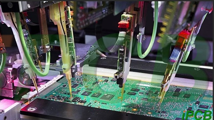
Quality control verifies that the manufactured PCB matches the approved design and technical specifications. Visual inspection and automated optical inspection can identify visible defects in circuit patterns, solder mask, and surface features. Electrical testing, including flying probe or fixture-based testing, checks for open circuits and short circuits to confirm that the conductive connections meet the design requirements.
For multilayer boards or designs with more demanding structural requirements, additional inspection methods may be appropriate. X-ray inspection can help examine internal structures, while microsection analysis provides a cross-sectional view of copper plating, via walls, and laminate construction. These methods are useful when internal quality needs to be verified more closely.
The inspection plan should reflect the board’s complexity and intended application. A straightforward two-layer PCB may not require the same testing as a high-density multilayer board. Manufacturers and customers should agree on the relevant acceptance criteria, inspection methods, and documentation before production begins.
How to Choose a Custom PCB Manufacturer
A suitable custom PCB manufacturer should have the equipment and process capabilities needed to produce the required board structure. Before placing an order, buyers should confirm the manufacturer’s supported layer count, material options, maximum and minimum board dimensions, copper thickness, trace width and spacing, via structures, and surface finishes.
Manufacturing experience is also important. A supplier familiar with similar PCB designs may be better prepared to identify fabrication risks and recommend practical adjustments. Buyers should review the manufacturer’s quality control procedures, electrical testing capabilities, production consistency, and ability to support both prototype and volume orders.
Communication during engineering review can also affect project efficiency. A manufacturer should be able to explain design limitations, clarify unclear specifications, and identify potential cost or lead-time implications before production. This helps reduce avoidable revisions and makes it easier to maintain consistency as the project moves from prototype to mass production.
Information Required for a Custom PCB Quote
To prepare an accurate quotation, manufacturers generally need the PCB design files and a clear set of technical specifications. Gerber files and drill data provide the information required for fabrication, while the layer stack-up, board thickness, copper weight, and surface finish define the board’s construction.
Order quantity, delivery requirements, and any special processing needs should also be included. If the design requires controlled impedance, high-current conductors, blind or buried vias, unusual materials, or specific inspection procedures, these requirements should be identified before the quotation is finalized. Complete information allows the manufacturer to evaluate the design more accurately and reduce the likelihood of changes after production starts.
What is the difference between a custom PCB and a standard PCB?
A standard PCB generally follows a predefined size or specification, while a custom PCB is manufactured according to the customer’s design files and technical requirements. Customization may involve board dimensions, layer count, materials, copper thickness, surface finish, and other manufacturing details.
Can I order a custom PCB circuit board in small quantities?
Yes. Many PCB manufacturers support prototype and small-batch production as well as volume manufacturing. Prototype orders allow engineers to evaluate the circuit design and mechanical fit before committing to larger production quantities.
Which material is best for custom PCB circuit boards?
FR-4 is suitable for many general-purpose applications, while high-Tg FR-4 and specialized laminates may be needed for more demanding thermal or electrical conditions. The best material depends on operating temperature, signal frequency, mechanical requirements, and manufacturing constraints.
How many layers can a custom PCB have?
The layer count depends on the manufacturer’s capabilities and the design requirements. Single-sided and double-sided boards are suitable for simpler circuits, while multilayer PCBs provide additional routing space for more complex designs.
How long does custom PCB manufacturing take?
Production time depends on board complexity, material availability, layer count, special processes, order quantity, and the manufacturer’s production schedule. Prototype orders with standard materials and specifications are generally simpler to process than complex multilayer boards with specialized requirements.
A custom PCB circuit board should be specified according to the needs of the finished electronic product rather than customized without a clear engineering purpose. Material selection, stack-up design, copper requirements, surface finish, and quality control all influence the board’s performance and manufacturing cost. By defining these requirements clearly and working with a manufacturer that can support the design, businesses can develop PCB solutions that are practical to produce and suitable for their intended applications.