Circuit board fabrication is the process of turning a PCB design into a physical bare circuit board that can later be assembled with electronic components. The process creates the copper traces, pads, vias, plated holes, insulating layers, solder mask, surface finish, and other physical structures defined by the design. Although the exact production route depends on the board type and its specifications, circuit board fabrication generally combines imaging, etching, lamination, drilling, copper deposition, plating, surface treatment, inspection, and electrical testing.
The circuit board fabrication process begins with digital manufacturing data rather than raw materials alone. Before production starts, the PCB design files are reviewed and converted into manufacturing instructions. The fabricator checks the layer structure, board outline, drill data, copper features, clearances, and other requirements to determine whether the design can be produced within the available process capabilities. This engineering stage is important because a PCB layout that is electrically correct in design software may still contain features that are difficult or costly to manufacture. Current PCB fabrication guidance consistently places DFM and manufacturing data preparation at the beginning of the production flow.
What Circuit Board Fabrication Actually Produces
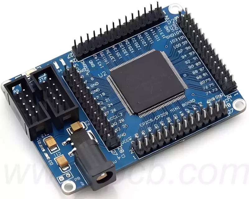
Circuit board fabrication produces the bare PCB, not the finished electronic assembly. The fabricated board contains the physical conductive and insulating structures needed to support electronic components, but components such as resistors, capacitors, integrated circuits, connectors, and sensors are installed during a separate PCB assembly process.
This distinction is important when discussing circuit board fabrication because PCB fabrication and PCBA manufacturing solve different problems. Fabrication establishes the board’s physical and electrical infrastructure, while assembly places and solders components onto that infrastructure. A bare board can therefore be fully fabricated and electrically tested without being a functioning electronic product until the required components are installed.
The final structure can vary considerably. A simple single-sided PCB may contain one conductive copper layer, while a multilayer circuit board can contain multiple internal signal, power, and ground layers separated by dielectric material. HDI boards can add microvias, fine-line circuitry, and sequential buildup structures when conventional interconnections cannot provide sufficient routing density.
Materials Form the Foundation of the Circuit Board
Most rigid circuit boards begin with copper-clad laminate. The material contains an insulating substrate and copper foil that becomes part of the electrical structure. FR-4 is widely used for general-purpose rigid PCBs, while other laminate systems can be selected when the design requires specific electrical, thermal, mechanical, or high-frequency characteristics.
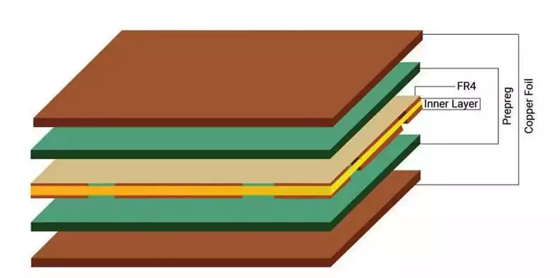
For a multilayer PCB, the material system includes cores, prepreg, and copper foil. These materials are arranged according to the required stack-up before being bonded together during lamination. The stack-up affects board thickness, layer spacing, impedance, copper distribution, and mechanical behavior, so it is part of the electrical design rather than merely a manufacturing detail.
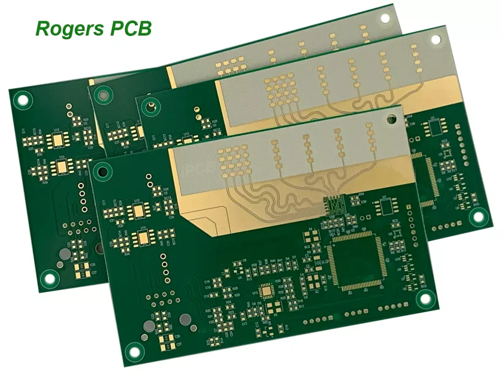
High-speed and RF boards require additional attention to material properties. Dielectric constant, dielectric loss, copper roughness, dielectric thickness, and dimensional stability can influence signal propagation and impedance. The material selected for fabrication therefore needs to match the requirements established during PCB design.
Inner Layer Fabrication Creates the Internal Circuits
For a multilayer circuit board, internal copper layers are normally formed before the complete stack is laminated. The copper surface is cleaned and coated with a photosensitive resist. The circuit image is then transferred to the panel using an imaging process, and the resist is developed to expose the copper that needs to be removed.
Chemical etching removes the unwanted copper and leaves the required traces, pads, planes, and other conductive features. The remaining resist is stripped after the circuit pattern has been formed.
This stage requires precise control because the internal layers will become inaccessible after lamination. Automated optical inspection can compare the manufactured pattern against the original design data and identify opens, shorts, missing copper, excessive copper, or other pattern defects before the layers are permanently bonded together.
The importance of this inspection increases with board complexity. Fine-line circuitry and tight spacing provide less tolerance for dimensional variation, while multilayer boards offer fewer opportunities to correct an internal defect after lamination.
Lamination Builds the Multilayer Structure
After the internal circuits have been fabricated and inspected, the individual layers are aligned and stacked with dielectric materials and copper foil. The stack is placed into a lamination press, where controlled heat and pressure cause the resin system to cure and bond the layers into a single structure.
Layer registration is critical during this stage. Every internal copper layer must remain aligned with the outer layers and the drilling coordinates that will be used later. A registration error can reduce the annular ring around a via, shift traces relative to pads, or create problems with fine-pitch components.
Lamination also determines the final dielectric structure between conductive layers. For controlled-impedance designs, changes in dielectric thickness can affect the electrical characteristics of transmission lines. This is why the fabricated stack-up should correspond closely to the stack-up used during PCB design and impedance calculations.
Drilling Creates the Mechanical Interconnections
Once the multilayer structure has been laminated, holes are drilled according to the manufacturing data. These holes can include component holes, plated through-holes, vias, mounting holes, and other mechanical features.
Mechanical drilling is widely used for conventional PCB holes, while laser drilling is used for certain smaller structures such as microvias in HDI fabrication. The drilling method depends on hole diameter, depth, aspect ratio, board construction, and the required interconnection technology.
Drilling is not simply a matter of creating openings in the laminate. Hole walls may contain resin residues and debris generated during the process. These contaminants need to be removed or treated before copper plating so that the hole walls can receive a reliable conductive layer.
Copper Plating Connects the PCB Layers
A drilled hole through a multilayer PCB initially passes through nonconductive dielectric material, so it cannot electrically connect the copper layers by itself. The hole wall must first receive a conductive copper coating.
The fabrication process commonly uses electroless copper deposition to establish an initial conductive layer inside the holes. Electrolytic copper plating can then build the required copper thickness on the hole walls and board surfaces. This creates the conductive path needed for plated through-holes and other interlayer connections.
Copper plating has both electrical and mechanical importance. The plated connection must maintain continuity between layers and withstand thermal and mechanical stresses during PCB assembly and operation. Hole geometry, aspect ratio, surface preparation, plating conditions, and copper thickness can all affect the reliability of the finished connection.
Outer Layer Fabrication Defines the Final Circuit
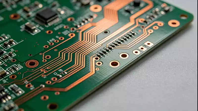
After drilling and initial copper deposition, the outer copper layers are patterned to create the traces and pads visible on the finished PCB. Photoresist and imaging processes define the required circuit pattern, followed by plating and etching processes that remove unwanted copper and preserve the intended conductive features.
The outer layers are particularly important because they interact directly with components during assembly. Pad dimensions, solderable areas, copper clearances, and via structures all need to remain within the tolerances required by the assembly process.
For high-density designs, outer-layer fabrication can become considerably more demanding. Fine-pitch packages may require narrow traces and small clearances, while via-in-pad and HDI structures can require additional process controls to maintain reliable connections.
Solder Mask Protects the Finished Circuit
Most of the exposed copper on a completed PCB is covered by solder mask. The coating provides electrical insulation between adjacent conductive features and protects copper from environmental exposure. Openings are created above component pads, test points, and other areas that need to remain accessible.
The solder mask process normally involves coating the board with a photosensitive material, exposing the required pattern, developing the coating, and curing it. The final mask opening must be accurately aligned with the underlying copper because excessive misregistration can reduce pad area or expose copper that should remain protected.
For fine-pitch PCB assembly, solder mask registration becomes increasingly important because the available space between adjacent pads is small. Fabrication tolerances therefore need to be considered together with the component land pattern and assembly requirements.
Surface Finish Protects Exposed Copper
After solder mask processing, exposed copper pads receive a surface finish. The finish protects the copper from oxidation and provides a suitable surface for soldering.
Common surface finishes include HASL, lead-free HASL, ENIG, OSP, and immersion silver. Each process has different characteristics related to surface flatness, solderability, environmental requirements, storage, and cost. The appropriate finish depends on the board’s component technology and assembly process rather than being selected independently from the rest of the PCB specification.
Fine-pitch components can place greater demands on surface flatness. For such designs, the choice of surface finish can influence assembly consistency and solder joint formation.
Profiling Produces the Final Board Shape
PCB fabrication usually takes place on larger production panels containing multiple circuit boards. After the main fabrication processes are completed, individual boards are separated from the panel using routing, punching, laser depanelization, or other suitable methods.
The final profile may contain straight edges, rounded corners, slots, cutouts, mounting holes, or other mechanical features. These features must correspond to the product enclosure and assembly equipment.
Board dimensions are particularly important for products with tight mechanical integration. A small difference in the PCB outline or the position of a mounting hole can prevent the board from fitting correctly into its enclosure, even when the electrical circuit itself is functioning properly.
Inspection Is Part of Circuit Board Fabrication
Inspection does not occur only at the end of fabrication. Quality control is distributed throughout the manufacturing process because some defects become difficult or impossible to correct after later stages.
Inner-layer AOI can identify circuit-pattern defects before lamination. After drilling and plating, inspection can verify hole quality and copper connections. Outer-layer inspection can check the final conductor pattern, while solder mask and surface-finish inspection can identify defects that could affect assembly.
Final electrical testing checks the connectivity of the manufactured PCB against the intended circuit. Depending on the product requirements, fabrication may also include dimensional inspection, visual inspection, microsection analysis, or other quality-control methods. Modern PCB fabrication workflows commonly combine optical, electrical, dimensional, and process-specific inspections rather than relying on a single final check.
Different PCBs Require Different Fabrication Processes
Circuit board fabrication is not identical for every PCB. A two-layer FR-4 board with standard through-holes has very different manufacturing requirements from an HDI board with microvias and fine-line circuitry.
A multilayer PCB adds internal layer fabrication and lamination. An HDI PCB may require sequential buildup, laser drilling, microvia formation, and additional registration control. Flexible and rigid-flex PCBs use different material systems and require fabrication methods that account for bending and mechanical movement. High-frequency PCBs can require specialized laminates and tighter control of dielectric thickness and copper surface characteristics.
Altium’s PCB fabrication education materials specifically distinguish standard rigid PCB fabrication from specialized processes used for flex, rigid-flex, and HDI boards.
This variation is one reason why a circuit board fabrication specification needs to describe the actual board requirements instead of relying on a generic statement such as “standard PCB.”
PCB Design Directly Affects Fabrication
A large part of fabrication success is determined before manufacturing begins. Trace width, spacing, hole diameter, annular ring, copper thickness, layer registration, board thickness, and impedance requirements all create manufacturing constraints.
For example, reducing trace width can increase routing density, but it also leaves less tolerance for imaging and etching variation. Reducing the via diameter can save board space, but smaller holes require more precise drilling and plating. Increasing the layer count can provide additional routing capacity, but it also adds lamination and registration complexity.
Designers therefore need to understand the fabrication process while developing the PCB layout. A design that fits comfortably within a fabricator’s process capability is generally easier to produce consistently than one that operates continuously at the edge of the process window. Current PCB fabrication guidance emphasizes this relationship between design rules, manufacturing capability, yield, cost, and production reliability.
Circuit Board Fabrication and DFM Work Together
Design for manufacturability is especially important before production because fabrication problems are cheaper to correct in digital design files than after panels have entered production.
A DFM review can identify insufficient clearances, unsupported hole sizes, unsuitable copper geometry, conflicting drill information, incorrect board outlines, and other potential manufacturing problems. The exact checks depend on the PCB technology and the capabilities of the fabricator.
The purpose of DFM is not to force every PCB into one standard design. Instead, it helps ensure that the intended design can be reproduced within a known manufacturing process. This becomes increasingly valuable for HDI, high-layer-count, high-frequency, heavy-copper, and other advanced PCB constructions.
What Makes Advanced Circuit Board Fabrication More Difficult
PCB fabrication becomes more challenging when several demanding requirements occur at the same time. A high-layer-count board may require tighter registration between many copper layers. A fine-line design reduces the available process margin. Small vias require greater drilling and plating precision. Heavy copper changes etching and plating requirements. High-frequency materials introduce additional concerns related to dielectric properties and dimensional stability.
These requirements can interact with one another. For example, a high-speed multilayer PCB may require controlled impedance, which depends on the relationship between trace geometry, copper thickness, dielectric thickness, and material properties. If the physical fabrication differs from the design assumptions, the finished transmission line may not achieve the expected impedance.
Advanced fabrication is therefore not simply a matter of adding more production steps. It requires tighter coordination between material selection, stack-up engineering, PCB layout, process capability, inspection, and testing.
Circuit Board Fabrication Determines More Than Appearance
The quality of a fabricated PCB cannot be judged only by its surface appearance. A board may look clean while still containing internal defects, poor plated-hole connections, dimensional errors, or electrical discontinuities.
The fabrication process determines the physical characteristics that the electronic assembly depends on. Copper thickness affects current carrying capability. Dielectric thickness influences impedance. Hole plating establishes interlayer connections. Surface finish affects solderability. Board dimensions determine mechanical compatibility.
For this reason, fabrication specifications should define the electrical, mechanical, material, and quality requirements that matter to the final application.
Circuit Board Fabrication Connects PCB Design With Production
Circuit board fabrication is the manufacturing stage that turns an electronic layout into a physical board capable of supporting components and electrical connections. It combines digital manufacturing data with materials, imaging, chemical processing, mechanical drilling, lamination, copper plating, finishing, and inspection.
The basic process is relatively consistent across many rigid PCBs, but the details change significantly with board complexity. Multilayer construction adds lamination and registration requirements. HDI introduces microvias and sequential buildup. High-frequency designs require tighter control of material and geometry. Flexible boards require fabrication methods suited to bending and mechanical movement.
Understanding circuit board fabrication helps engineers create designs that are not only electrically functional but also manufacturable. When PCB design rules, material selection, stack-up, fabrication capability, inspection, and testing are considered together, the finished board is more likely to meet its intended electrical and mechanical requirements.