A bare PCB serves as the core framework of a traditional circuit board; its fundamental function is to guide the flow of current through carefully designed circuit paths, and it is widely used in various types of electronic devices. A blank PCB (i.e. a bare board) features a simple structure, offering engineers and designers ample design freedom and allowing them to flexibly add electronic components according to actual requirements. It combines a high degree of flexibility with excellent suitability for mass production.
Compared to other wiring methods, the initial design work for bare PCBs is more complex; however, once manufacturing and assembly are complete, subsequent production can be automated, making it the most cost-effective and efficient wiring solution for electronic devices. It should be noted that bare PCBs do not possess any practical functionality in themselves; only after being fitted with the appropriate components can they become complete circuit boards suitable for various applications. Furthermore, blank PCBs represent the optimal stage for conducting bare board testing during the circuit board manufacturing process, which is crucial for preventing various issues during subsequent production and use.
Main classifications of bare PCBs
Bare PCBs can be classified according to four key dimensions: number of structural layers, substrate material, substrate properties, and environmental compliance rating. Different categories are suitable for different scenarios.
Classification by Number of Layers
Single-sided PCB: Only one side features a conductive copper layer, whilst the other side consists of an insulating substrate. This is the simplest structure and the lowest cost option, suitable for circuits with low line density and simple functions.
Double-sided PCB: Both sides feature conductive copper layers, with an insulating substrate sandwiched in between; the upper and lower layers are connected via through-holes. Currently the most widely used and offering the best value for money, this type is suitable for most conventional electronic devices.
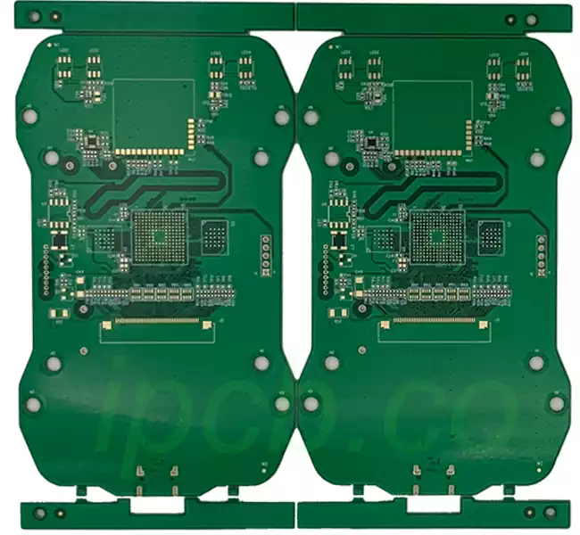
Multilayer boards: Composed of three or more conductive layers laminated together, with inter-layer connections via buried, blind or through-holes. Primarily used in equipment with high circuit density, stringent performance requirements and complex structures, such as computer motherboards, telecommunications equipment and high-end power adapters.
Classification by substrate material
Rigid boards: The most common type of PCB, manufactured using rigid substrates, primarily including:
FR-4: The most widely used type, utilising glass fibre cloth as the reinforcing material and epoxy resin as the binder. It offers a balanced combination of electrical and mechanical properties and is suitable for the vast majority of standard electronic devices.
Metal-core PCBs: These use a metal core (typically aluminium) as the substrate, combined with an insulating layer and copper foil. They offer excellent heat dissipation and are primarily used in applications with high thermal requirements, such as LED lighting and high-power power adapters.
High-frequency and high-speed boards: Such as the Rogers series and PTFE (polytetrafluoroethylene) substrates. These offer excellent dielectric properties and low signal loss, making them suitable for RF/microwave equipment and high-speed signal transmission.
Ceramic substrates: Made from ceramic materials such as aluminium oxide, these offer excellent thermal conductivity and insulation, as well as high stability, making them suitable for high-power and high-temperature operating environments.
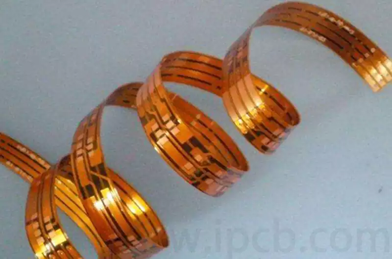
Flexible Printed Circuits (FPC): Manufactured using bendable flexible substrates (such as polyimide (PI)), these primarily include:
Single-sided FPC: A single layer of copper foil paired with a PI substrate; with a simple structure, it is suitable for small, bendable, and simple circuits.
Double-sided FPC: Two layers of copper foil sandwiching a PI substrate and laminate layers, with through-holes connecting the circuits on both sides; suitable for flexible circuits of medium complexity.
Multi-layer FPC: Composed of three or more conductive layers laminated together, enabling complex flexible circuit layouts; used in high-end flexible electronic devices.
Rigid-flex boards: Combining the characteristics of rigid and flexible boards through specific manufacturing processes, these are suitable for space-constrained applications requiring both rigid mounting and flexible bending, such as precision instruments and portable electronic devices.
Classification by substrate properties
Standard boards: Performance meets general requirements, offering high value for money and the most common type.
High Tg boards: Featuring a high glass transition temperature and excellent heat resistance, these are suitable for applications involving high soldering temperatures or high ambient operating temperatures, such as industrial equipment and high-end power supplies.
Halogen-free boards: The substrate contains no halogen elements such as bromine or chlorine, making them highly environmentally friendly and compliant with modern environmental standards.
High-frequency boards: Featuring low dielectric constant and low loss factor, they ensure stable transmission of high-frequency signals and are suitable for RF and microwave equipment.
High-speed boards: With low dielectric constant and low loss, they prioritise signal integrity and impedance control, and are specifically designed for high-speed digital signal transmission, such as in servers and high-end communication equipment.
Classification by Environmental Standards
RoHS-compliant boards: Conform to the EU RoHS Directive, strictly limiting the use of hazardous substances such as lead and mercury; currently the mainstream type of environmentally friendly PCB.
Lead-free tin-plated boards: Treated with lead-free solder on the surface, compatible with lead-free soldering processes, meeting environmental and electronic equipment reliability requirements.
Why is bare PCB testing necessary?
As the ‘backbone’ of a circuit board, the quality of a bare PCB directly determines the reliability of the final assembled circuit board. Although the probability of defects occurring in bare PCBs during production is low, issues such as over-etching, under-etching and voids may still arise; even minor defects can lead to assembly failures or equipment malfunctions later on.
As electronic devices become increasingly miniaturised and high-density, the demand for multilayer PCBs is growing. Once assembled, multilayer boards are virtually impossible to repair if faults occur, making bare board testing all the more crucial. Furthermore, electronic components are typically expensive and play a critical role; testing bare boards in advance to create a ‘robust framework’ can effectively prevent the wastage of high-end components due to bare PCB defects, thereby significantly reducing repair and replacement costs in the long term.
Key Benefits of Bare PCB Testing
Bare PCB testing has virtually no significant drawbacks; a modest investment during the manufacturing process can avert a host of potential issues later on. Its key benefits include:
Early detection and root-cause resolution: Bare PCB testing identifies defects at an early stage of manufacturing, facilitating rapid root-cause identification and thorough resolution. If problems are only discovered during component assembly or final product debugging, not only is it difficult to pinpoint the root cause, but rectification costs also increase.
Avoiding confusion over faults and simplifying troubleshooting: Once components are mounted on the PCB, the cause of a fault may lie with either the bare board or the components themselves. Early bare board testing can rule out potential issues with the bare board in advance; should faults arise later, the focus can be directed straight to the components, significantly simplifying the process.
Ensuring Smooth Production and Improving Efficiency: By resolving all issues through bare board testing during the prototype development stage, downtime and rework caused by bare board defects can be avoided during subsequent mass production, ensuring a smooth production process and improving overall efficiency.
Bare PCB Board Testing Methods
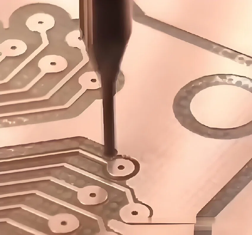
1.AOI Testing (Automated Optical Inspection)
AOI testing utilises high-precision cameras to capture images of the bare PCB. Through image processing technology, these images are compared against standard templates to automatically identify defects in areas such as pads, traces and silkscreen (e.g. poor etching, scratches, foreign objects). Its advantages include high testing speed, accuracy and repeatability, with no need for manual intervention. It is highly suitable for rapid screening on large-scale production lines and is currently the most commonly used bare PCB testing method in mass production.
2.Fly-Probe Testing
Fly-probe testing is a contact-based inspection method that utilises fine probes to sequentially contact test points on the bare PCB. By measuring circuit continuity, it accurately determines the presence of electrical defects such as open circuits or short circuits. This method offers extremely high precision and is particularly suitable for multilayer boards or high-precision circuit boards with complex circuits and small test spacing; however, its testing speed is relatively slow, making it more suitable for testing small batches of high-precision products, samples, or customised PCBs.
3.Fixture Testing
Fixture testing requires the prior design of a dedicated test fixture, where the probes on the fixture correspond one-to-one with the test points on the bare PCB. Once connected to the test equipment, multiple electrical performance parameters can be tested simultaneously. Its advantages include high testing accuracy, strong stability and high efficiency, making it suitable for mass production and products with customised testing requirements, whilst significantly improving the efficiency and consistency of batch testing.
4.Manual Visual Inspection
Visual inspection is the most intuitive testing method, in which experienced staff use the naked eye or a magnifying glass to observe obvious defects on the surface of the bare PCB (such as scratches, foreign objects, unclear silkscreen printing, or damaged pads). The speed and accuracy of this method are significantly influenced by the inspector’s experience and fatigue levels, and its precision is limited. It is typically used as a supplement to automated testing and is suitable for small-batch production, specialised custom products, or as an auxiliary inspection for simple single-sided boards.
Although bare PCBs do not directly contribute to circuit functionality, their quality determines the reliability of the entire electronic product. From appropriate classification and selection to thorough testing and verification, every step warrants careful attention.