In printed circuit board (PCB) design, pcb thickness is a crucial parameter. Currently, 1.6 mm is the most commonly used standard thickness in the vast majority of general-purpose applications, such as consumer electronics and industrial control. However, as electronic products evolve towards miniaturisation, high performance and multifunctionality, PCB thickness must also be selected flexibly according to specific application scenarios. The following outlines common PCB thickness classifications and their applicable fields.
Common PCB Thickness Categories and Applicable Scenarios
1.Ultra-thin Boards (0.4mm, 0.6mm, 0.8mm)
Primarily used in applications where space is extremely limited, such as flexible printed circuits (FPCs), wearable devices (smartwatches, fitness trackers), mobile phone camera modules, and internal circuits of TWS earphones.
Characteristics: Extremely thin, allowing for bending or adaptation to irregular shapes, but requiring high standards in manufacturing processes and materials.
2.Standard Thin Boards (1.0mm, 1.2mm)
Suitable for compact devices that do not require extreme flexibility, such as routers, Internet of Things (IoT) sensor modules, smart home controllers, and portable medical devices.
Compared to ultra-thin boards, these offer lower costs whilst still meeting the mechanical strength requirements for most low-to-medium power applications.
3.Industry-standard thickness (1.6mm)
The most widely used thickness, offering a balance of mechanical strength, thermal dissipation, manufacturing yield and universal compatibility.
Typical applications: Computer motherboards, power supply adaptor boards, household appliance control boards, industrial automation control boards, general-purpose prototype development boards, etc.
4.Thick Boards / High Reliability Requirements (2.0mm, 3.0mm and thicker)
Used in environments involving high current transmission, high heat generation or high mechanical stress, such as high-power power supply modules, server backplanes, telecommunications base station equipment, and automotive electronics (certain ECUs).
Thicker substrates facilitate the use of thicker conductors (or thicker copper foil), whilst enhancing resistance to vibration and impact.
Thickness Characteristics of Special-Type PCBs
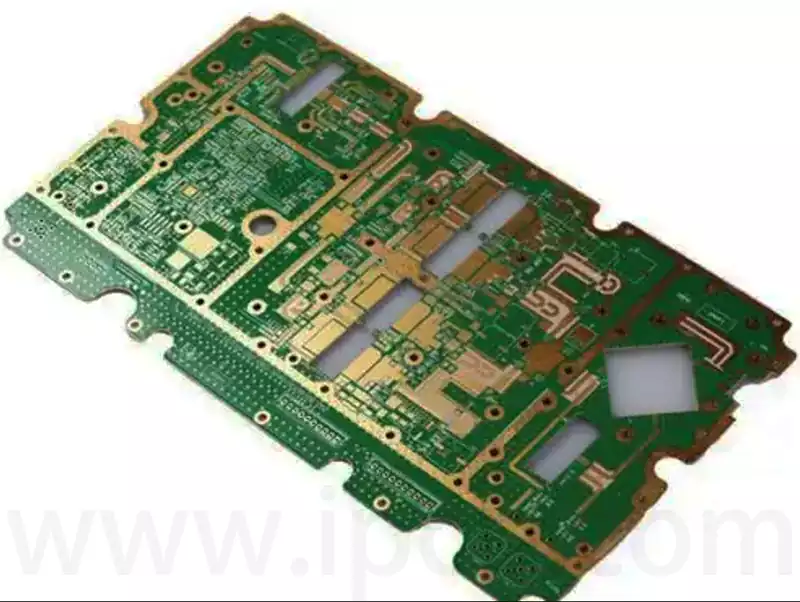
Multilayer board stack-up structure: Formed by alternately laminating core material and prepreg (PP sheets), with total thicknesses ranging from 0.4 mm to 6 mm or more. For example, in high-speed digital boards or RF boards with 12 or more layers, the stack-up thickness often needs to be precisely controlled to ensure signal integrity and interlayer impedance matching.
Metal-based substrates (e.g. aluminium substrates, copper substrates): Primarily used in high-power LED lighting, power supply modules and motor drive circuits. Common thicknesses range from 1.0 mm to 3.0 mm, with the metal layer providing an excellent heat dissipation path, whilst the thickness of the insulating layer is adjusted according to voltage withstand requirements.
Rigid-flex boards: Combine the characteristics of both rigid and flexible boards. The flexible regions can be as thin as 0.1–0.3 mm to allow for bending or dynamic flexing; the rigid regions have the same thickness as conventional PCBs (e.g. 1.6 mm) and are used for component mounting.
The impact of PCB thickness on circuit board performance
1.Electrical performance and current-carrying capacity
PCB thickness directly affects the cross-sectional area of the conductive layer (copper foil). Under identical trace width conditions, a thicker PCB (particularly when paired with thicker copper foil) can carry a higher current due to its lower resistance and reduced temperature rise. For high-power equipment (such as motor drivers and switching power supplies), it is common practice to select a board thickness of 2.0 mm or even 3.0 mm, combined with 2 oz or thicker copper foil. Conversely, in high-speed digital or high-frequency RF circuits, thinner PCBs (such as 0.8 mm or 1.0 mm) help to shorten signal return paths and reduce parasitic inductance and capacitance, thereby minimising signal attenuation and electromagnetic interference (EMI).
2.Thermal Management Capabilities
PCB thickness (particularly copper foil thickness and the substrate’s thermal conductivity) has a significant impact on heat dissipation performance. Thicker copper layers can more effectively conduct heat from heat-generating components (such as power MOSFETs, processors and LEDs) across the entire board surface, before dissipating it via a heat sink or natural convection. If the copper foil is too thin or the substrate is too thick but has poor thermal conductivity (for example, standard FR-4 material has a thermal conductivity of only approximately 0.3 W/m·K), heat is likely to accumulate, leading to increased junction temperatures in components, accelerated ageing, and even failure. For high-power-density designs, metal substrates or thick PCBs with built-in thermal conductive layers may be selected.
3.Mechanical Strength and Reliability
Strength and Rigidity: Thicker PCBs generally possess higher bending stiffness and torsional strength, making them suitable for equipment requiring plug-in connectors, the installation of large heat sinks, or exposure to vibration and shock (such as automotive electronics and industrial control cabinets). However, excessively thick boards (e.g. >3 mm) increase the difficulty of drilling, edge milling and lamination, and may lead to misalignment of the inner layers.
Flexibility Requirements: For wearable or foldable screen devices, ultra-thin boards (0.4 mm or even thinner) or flexible boards are essential; these sacrifice some mechanical strength in exchange for the required bending endurance.
Risk of processing defects: During the lamination of multilayer boards, if the total thickness is excessive and the coefficients of thermal expansion of the individual layers are inconsistent, defects such as interlayer slippage, bubbles and resin voids are likely to occur, thereby reducing yield and long-term reliability.
4.Cost and production process complexity
Material Costs: Thicker substrates (e.g. 2.0 mm and above) have a higher unit cost. Furthermore, if thick copper (e.g. 3 oz or more) is required, the cost of copper foil increases significantly.
Processing Costs: Drilling thicker boards accelerates drill bit wear, necessitating improved chip removal and cooling measures; etching thick copper requires longer etching times, making side etch control more difficult, which affects the ability to achieve fine line widths and spacing.
Yield Rate: Extremely thin boards (≤0.4mm) are prone to warping or damage during handling, component placement and reflow soldering. They impose special requirements on jigs and vacuum cups for automated production lines, which also affects overall costs.
How to select the appropriate PCB thickness?
Designers must strike a balance between electrical performance, thermal management, mechanical strength, manufacturability and project budget:
Prioritise 1.6 mm as the default starting point, unless there are explicit space, current or thermal constraints.
For portable, lightweight and slim products, opt for 0.8 mm to 1.2 mm.
For high-current or high-reliability applications, consider 2.0mm or greater, potentially in combination with metal substrates or thick copper foil.
In high-frequency, high-speed circuits, simulation tools should be used to determine the optimal thickness (thinner is generally preferable), whilst strictly controlling the laminate structure.
By selecting the PCB thickness scientifically, one can ensure stable and reliable product performance whilst effectively managing manufacturing complexity and costs.