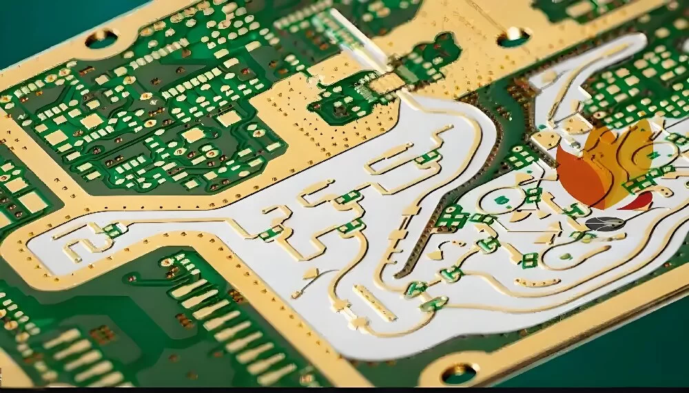
PCB board assembly processing, there may be a variety of defects, these defects can be categorised as the following major aspects, designed to improve product quality and reduce the defective rate.
Welding defects
Welding is a key part of PCB board assembly processing, common welding defects include:
False soldering (Dry Joints/Cold Solder): refers to incomplete solder joints or weak soldering, which may lead to circuit breakage or instability. This is usually indicated by a distinct black boundary between the solder and the component leads or copper foil, with the solder recessed towards the boundary. False soldering can also occur because there is not enough solder on the surface of the joint.
Cold Solder (Cold Solder): Insufficient soldering temperature, the solder is not completely melted, resulting in white solder joints, no metallic luster and rough surface. In the parts of the tin eating interface does not form the tin eating band, that is, bad solder.
Solder Bridge/Bridging: An unwanted connection between two or more solder joints that results in a short circuit. This can be caused by incorrect solder paste application or too much solder.
Non-Wetting: The solder is not coated with tin and the part and substrate are not soldered together. Reasons for this may include unclean pads, high soldering pins, poor solderability of the part, shifting of the part, or improper dispensing resulting in overflow of solder. Empty soldering means that there is tin on the pad but no tin on the component, and there is no contact between the two, resulting in a complete disconnection.
Tin beads (Solder Ball): Solder joints form small ball-shaped particles that adhere themselves to the surface of the PCB board or solder resist. Usually caused by too much solder paste, poor solder paste printing or improper soldering temperature.
Excess Solder: Excessive solder on a solder joint can lead to short circuits or unstable connections. Too much solder will make the component solder ends and pins surrounded by solder, or the middle of the solder joint contains air bubbles, which may lead to non-wetting and the risk of bridging.
Insufficient Solder: Too little solder on the solder joints may result in insufficient strength or poor conduction, even intermittent breaks.
Tombstoning: Surface mount components (such as resistors or capacitors) warp at one end during the soldering process, resembling a tombstone. This is usually due to asynchronous solder melting times at both ends of the component, different surface tensions, poor pad design, or temperature profile settings.
Voids/Blowholes: Air bubbles in a solder joint that affect solder reliability. Pinholes are small holes in a solder joint, and blowholes are larger holes in a solder joint that can be seen from the inside, usually caused by the solidification of solder when the gas is not completely expelled.
Pad Lifting: Solder joints peel off from the copper foil, usually due to excessive soldering time, high temperature or excessive force on the pad.
Solder Cracks: Cracked or loose appearance of solder joints, which may be caused by quality and freshness of solder paste or improper storage conditions.
Component Placement Defects
Component placement is a core step in SMT (Surface Mount Technology) processing and common defects include:
Misaligned/Offset Components: Components are not accurately placed on the pads, which can result in poor contact, inaccurate soldering or unstable electrical connections. Causes may include misalignment of the placement machine, uneven solder paste printing, or ambiguous positioning datums.
Missing Components: Certain components are missing from the PCBA, resulting in an incomplete circuit. This may be due to poor vacuum pump performance resulting in insufficient vacuum or suction nozzle problems.
Wrong Polarity/Flipped Components: Polarised components are mounted backwards or components are flipped, resulting in functional failure.
Substrate Defects
Defects can also be caused by the quality of the PCB board assembly substrate itself:
Substrate Warpage (Board Warpage): Bending or twisting of the substrate during the production process, which may be caused by uneven substrate material, improper heat treatment or production process problems. Warpage can lead to uneven soldering and cracked solder joints.
Delamination: Separation between PCB layers.
Blistering (Blistering): Bubbles appear on the surface of the substrate, usually caused by the separation of resin and fibres.
Short Circuit (Short Circuit): the circuit board should not be connected to the two solder joints by the solder accidentally connected.
Open Circuit (Open Circuit): The solder joints are not successfully connected, resulting in an electrical open circuit.
Pad Lift-off: Separation of the substrate pads from the substrate, usually due to thermal or mechanical stresses during the soldering process.
Hole Defects (Hole Defects): such as through-hole open-circuit, may be the manufacturing process residual etching solution is not removed, long-term corrosion of the through-hole wall caused.
Printing Defects
Solder paste printing is the first process of surface mount technology (SMT), the printing quality directly affects the subsequent soldering:
Uneven Solder Paste Printing (Uneven Solder Paste Printing): The amount of solder paste is too much or too little, affecting the quality of soldering.
Printing offset (Solder Paste Misalignment): Solder paste is not accurately printed on the pad, which may lead to poor soldering or solder paste misalignment.
Insufficient Solder Paste (Insufficient Solder Paste): solder paste is not on the pad, resulting in incomplete printing.
Pulling the tip (Solder Paste Spikes): After the solder paste is printed, there are sharp protrusions of solder paste on the pads.
Collapse (Slump): the appearance of the solder paste graphic defects, refers to the solder paste printing graphic mutilation or depression.
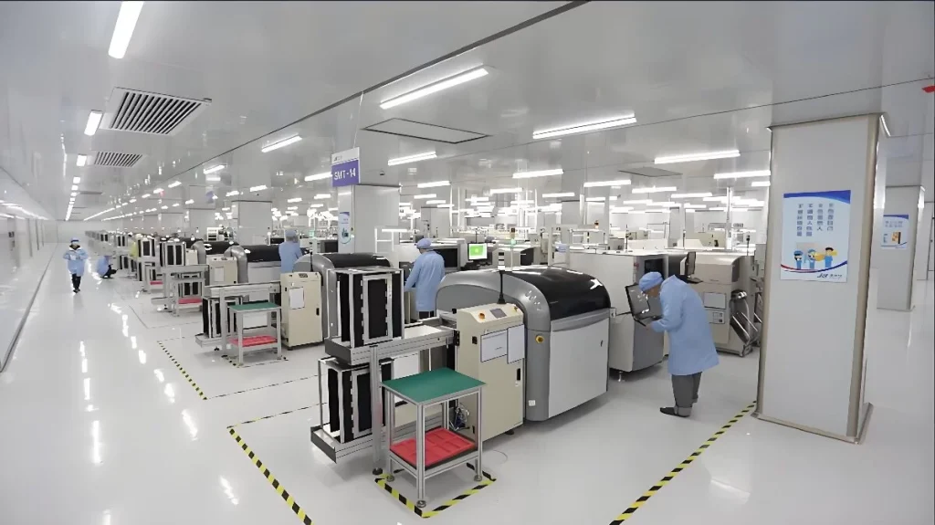
Test and Inspection Defects
Problems may also be found or generated during testing and inspection in the later stages of PCBA production:
Functional Test Failure (Functional Test Failure): PCB board assembly does not work as expected, may be due to component damage, soldering problems or design errors.
Visual Inspection Omission (Visual Inspection Omission): Manual visual inspection may not be able to find all the defects, especially small or hidden defects.
Defect Classification: Depending on their impact on the product, defects are usually classified as Major Associated Defects (MA), which may cause damage to the product, abnormal functionality, or affect the life of the product, and Minor Associated Defects (MI), which do not affect the functionality of the product.
Other defects
In addition to the above categories of major defects, PCB board assembly processing may also occur:
Pollution (Contamination): The presence of contaminants on the surface of the PCB board assembly will interfere with solder flow and wetting, increase soldering defects, and may reduce electrical performance.
Solder slag (Solder Dross): metal residues generated during soldering, which may affect the connectivity and stability of the solder joints.
Soldering Stress (Soldering Stress): In the soldering process, if the material is subjected to excessive thermal or mechanical stress, it may lead to cracking of the solder joints or pads, affecting the stability and life of the circuit.
Various types of defects in PCBA processing directly affect product performance and reliability. To achieve high-quality manufacturing, the key lies in the accurate identification, effective prevention and continuous improvement of these defects. By optimising the process, introducing advanced testing technology and continuously improving the quality management level, enterprises can significantly reduce the defective rate, thus ensuring the excellent performance and reliability of PCB board assembly products.