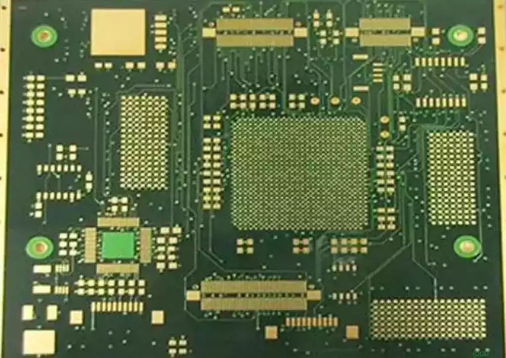
In PCB design, 1oz (ounce) and 2oz are common units for measuring copper foil thickness, with 1oz approximately equating to 35 micrometres (μm). The selection of copper thickness is not arbitrary; it directly impacts the circuit board’s current-carrying capacity, thermal dissipation performance, manufacturing costs, and suitability for specific applications. It stands as one of the key factors determining product performance and reliability.
Core Parameter Comparison Between 1oz and 2oz Copper Thickness
| Comparison Dimension | 1oz Copper Thickness (≈35μm) | 2oz Copper Thickness (≈70μm) | Differential Analysis |
| Cross-sectional area | Smaller | Larger (approximately twice that of 1oz) | The 2oz copper doubles the cross-sectional area, laying the foundation for reduced resistance. |
| Resistance Value | Higher (approximately double that of 2oz) | Lower (approximately half that of 1oz) | Resistance is inversely proportional to cross-sectional area; 2oz exhibits lower energy loss. |
| Current Carrying Capacity | Lower (suitable for small to medium currents) | Higher (suitable for medium to high currents) | At the same line width, the current carrying capacity of 2oz is nearly double that of 1oz. |
| Temperature Rise Performance | Higher temperature rise at equivalent current | Lower temperature rise at equivalent current | 2oz: Lower resistance, reduced heat generation, superior heat dissipation capability. |
| Manufacturing Cost | Lower (reduced material usage, mature processes) | Higher (material cost +20%–30%, complex processes) | 2oz: Significantly increased cost with heightened manufacturing precision requirements. |
| Processing Difficulty | Low (mature processes such as etching and drilling) | High (requires adjustment of etching, plating, lamination parameters, etc.) | 2oz prone to issues like line width deviation and rough hole walls. |
The Decisive Influence of Copper Thickness on Current-Carrying Capacity
The essence of current-carrying capacity lies in a conductor’s ability to withstand the heat and losses generated when carrying electrical current. The core factor determining this capacity is the cross-sectional area of the copper foil. When the copper layer thickness increases from 1oz to 2oz while maintaining the same trace width, the cross-sectional area of the copper foil nearly doubles. The most direct consequence of this change is a significant reduction in trace resistance.
According to the formula for copper resistivity, under identical trace length and ambient temperature conditions, a larger cross-sectional area results in lower resistance to current flow and reduced energy dissipation. Specifically, the trace resistance of 1oz copper thickness is approximately double that of 2oz copper thickness. This implies that under identical current conditions, 1oz copper foil generates substantially more heat than 2oz copper foil.
Referencing the current-carrying capacity reference data from the IPC-2152 standard, under identical line width and temperature rise conditions, the current-carrying capacity is broadly proportional to the copper thickness. For instance, a 1oz copper foil trace with a 10mil width can reliably carry 1-1.5A at a 25°C temperature rise, making it suitable for low-to-medium current applications.
Conversely, a 2oz copper foil trace of the same width can handle 2.5-3A, adequately meeting the demands of medium-to-high current transmission (5-15A). This disparity becomes particularly pronounced in high-power equipment. Within a 12V input, 8A output power module, traces using 1oz copper thickness readily exhibit significant heating, potentially compromising the stability of surrounding components. Conversely, 2oz copper thickness ensures stable current transmission by reducing resistance and dissipation.
Naturally, the enhancement of current-carrying capacity with increased copper thickness is not strictly linear. Practical applications are further influenced by factors such as trace width, ambient temperature, and heat dissipation conditions. Nevertheless, it remains undeniable that upgrading from 1oz to 2oz copper thickness remains one of the most direct and effective methods for bolstering a PCB’s current-carrying capability.
Cost and Process Challenges Posed by Copper Thickness
Increased copper layer thickness inevitably leads to higher costs—a fundamental principle in PCB manufacturing and a critical factor engineers must weigh during component selection. The manufacturing cost of a 2oz copper PCB is approximately 20% to 30% higher than that of a 1oz copper PCB, with specific variations depending on product specifications, production batch size, and process requirements.
From a material cost perspective, copper—as the core raw material for PCBs—directly impacts overall manufacturing expenses. The copper foil consumption for a 2oz copper thickness doubles that of a 1oz thickness, increasing material costs alone by 10% to 18%. Should copper market prices fluctuate significantly, this disparity may widen further.
The rise in processing costs is equally significant. The greater hardness of 2oz copper foil substantially increases process complexity during etching, drilling, and lamination:
During etching, thicker copper foil requires extended processing times and more precise parameter control. Failure to achieve this may result in incomplete etching or line width deviations, increasing the risk of product scrap.
When drilling, thicker copper foil accelerates drill bit wear, reduces processing efficiency, and necessitates adjusted drilling parameters to prevent copper foil flaking from the hole walls.
During lamination, thick copper foil demands higher flatness standards, necessitating optimised temperature and pressure settings to prevent interlayer separation, voids, and other defects.
Precision Control in Manufacturing Processes
The core of PCB manufacturing lies in precise process control. Increasing copper layer thickness from 1oz to 2oz represents far more than a simple material upgrade; it constitutes a comprehensive challenge to the entire production workflow.
The etching process is pivotal for controlling trace precision. For 2oz thick copper foil, traditional 1oz etching parameters become obsolete. Thicker copper etches more slowly; maintaining original etch times risks copper residue along trace edges, while excessive prolongation may cause traces to become excessively thin or even break. Consequently, adjustments to etchant concentration, temperature, and etch rate are required, alongside optimised exposure parameters, to ensure trace precision meets design specifications.
Through-hole plating processes likewise require targeted optimisation. For PCBs with 2oz copper thickness, the copper layer thickness on the inner walls of through-holes demands higher specifications, typically requiring 20 to 25μm (meeting IPC Class 2 or higher standards). This necessitates adjusting electroplating parameters, extending plating time, and optimising current density to ensure uniform plating on through-hole inner walls without voids. Furthermore, drilling thick copper foil increases hole wall roughness, necessitating optimisation of hole wall treatment processes to prevent poor adhesion between the plating and hole walls.
Beyond etching and via plating, processes such as lamination and solder resist application also require corresponding adjustments. During lamination, temperature, pressure, and time must be optimised to ensure robust interlayer bonding. For solder resist application, coating thickness and curing parameters need adjustment to prevent copper exposure or solder resist delamination. These process modifications rely not only on extensive manufacturing expertise but also on a robust quality control system to guarantee the manufacturability and yield of 2oz thick copper PCBs.
The choice between 1oz and 2oz copper thickness fundamentally represents a comprehensive trade-off between performance, cost, and process feasibility. For cost-sensitive products with lower current demands, such as consumer electronics, 1oz copper thickness offers superior value for money through its mature processes and economical cost, achieving an optimal balance between performance and expenditure.
Conversely, in demanding applications such as high-power supplies, industrial control systems, automotive electronics, and renewable energy equipment—where stringent current transmission and reliability are paramount—the cost increment associated with 2oz copper thickness often yields superior current-carrying capacity, enhanced thermal dissipation, and extended product longevity. From a full lifecycle perspective, this approach frequently delivers greater overall value for money.