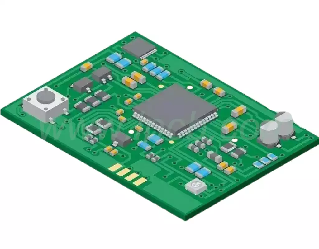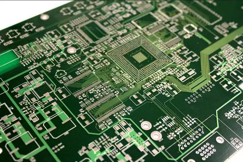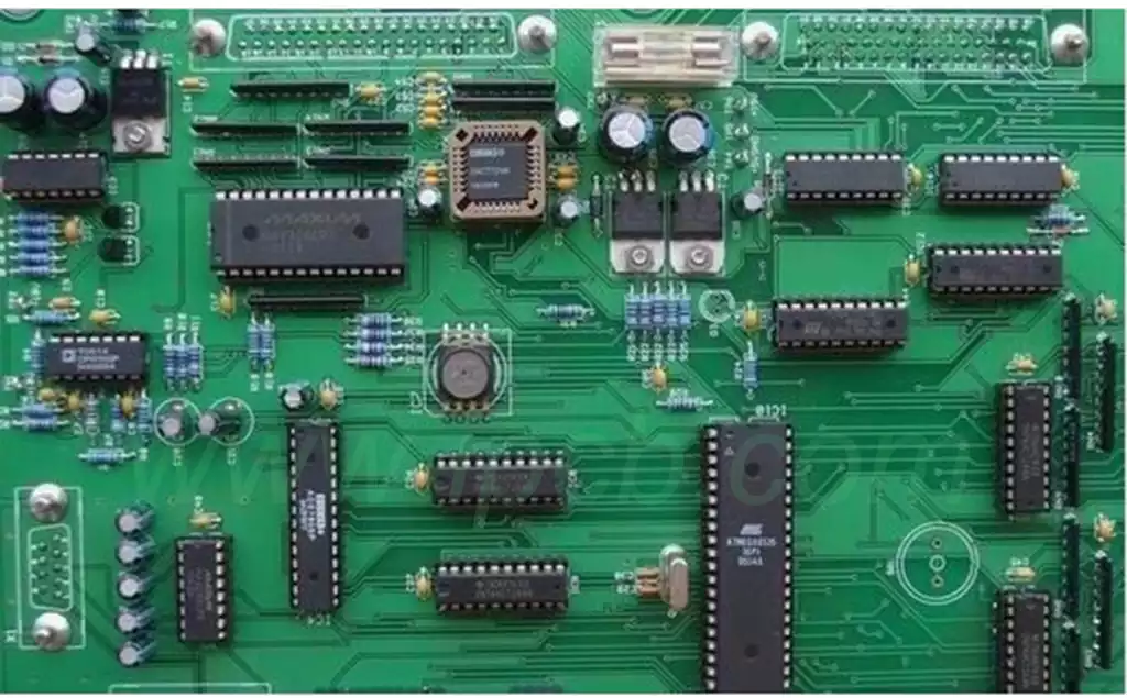
In the grand landscape of modern electronics industry and printed circuit board (PCB) design, if microprocessors and integrated circuits are the “intelligent brain” of the entire system, then various semiconductor diodes are the “unsung heroes” who safeguard system safety, maintain current order, and achieve energy conversion and logic rectification. From the fleeting electrostatic discharge (ESD) protection at smartphone charging ports to the ceaseless freewheeling rectification within high-power industrial switching power supplies, diodes are ubiquitous.
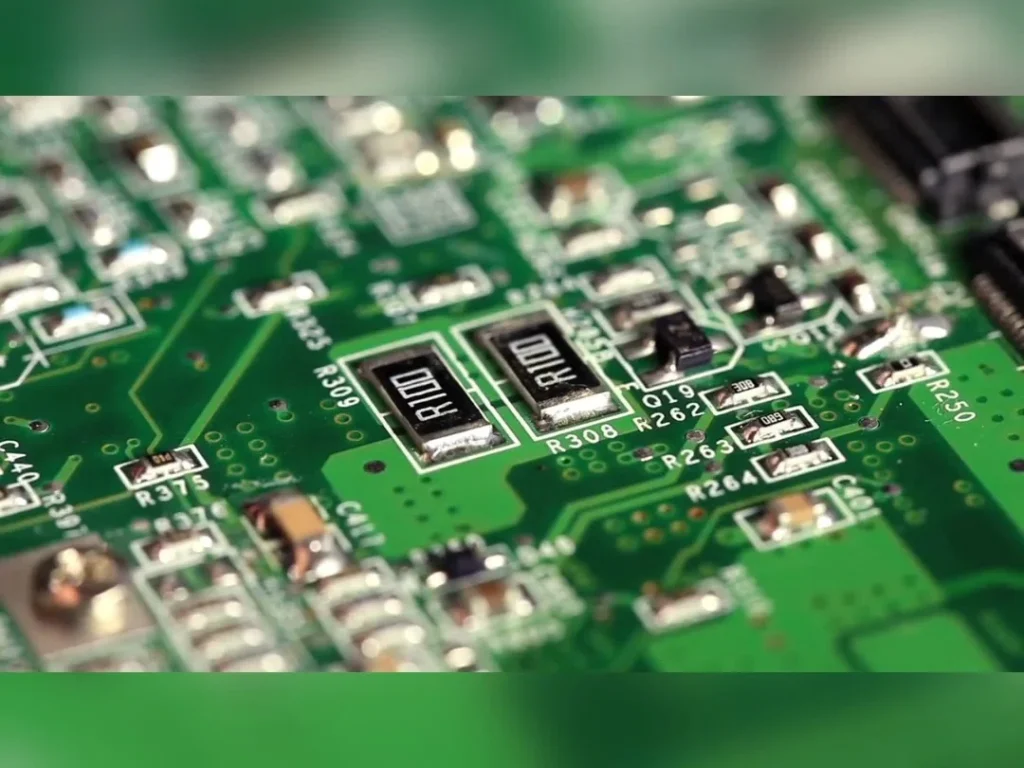
However, in the high-speed, high-density, and high-power-density demands of modern PCB design, diode pcb are far more than just simple unidirectional conductive symbols on schematics. Perfectly integrating and soldering a diode onto a PCB involves a deep interplay of multiple disciplines, including semiconductor solid-state physics, thermodynamics, electromagnetic compatibility (EMC), and micro-metallurgy. Understanding the physical behavior, failure mechanisms, and layout topology of diodes in a PCB environment is a core competency that every senior hardware engineer and electronics manufacturing expert must master.
Semiconductor Nature and Diode Topology Classification on Circuit Boards
To deeply understand the engineering applications of diodes on printed circuit boards, we must first peel back their physical shell and examine their microscopic semiconductor nature, composed of a PN junction.
The Unidirectional Conductivity Mechanism of a PN Junction
The core of a diode is a PN junction formed by the tight bonding of P-type semiconductors (rich in holes) and N-type semiconductors (rich in free electrons). When a forward voltage is applied to the anode and a negative voltage to the cathode, the applied electric field weakens the built-in electric field within the PN junction, causing carrier diffusion and resulting in a large forward current. At this time, the diode exhibits extremely low resistance.
Conversely, when a reverse voltage is applied, the applied electric field and the built-in electric field are aligned, the depletion layer widens sharply, blocking the free movement of carriers. Only a very small reverse leakage current flows, and the diode exhibits an extremely high impedance insulating state. It is this inherent unidirectional conductivity that makes it an irreplaceable current valve on printed circuit boards.
Common Diode Family Tree on PCBs
Depending on the circuit’s functional requirements, engineers deploy various types of diodes on circuit boards:
Rectifier Diode: Typically operates at the input of low-frequency AC-to-DC power supplies, possessing extremely high forward surge current withstand capability and high reverse voltage withstand.
Schottky Diode: Utilizes a potential barrier formed by the metal-semiconductor contact instead of a traditional PN junction. Its greatest physical advantages lie in its extremely low forward voltage drop and ultra-fast switching recovery speed, making it widely used in the output rectification and freewheeling circuits of high-efficiency DC-DC switching power supplies.
Zener Diode (Zenitr Diode): Specifically designed to operate in the reverse breakdown region. When the reverse voltage reaches a specific threshold, its terminal voltage remains constant, often used for generating local reference voltage sources and overvoltage clamping protection on circuit boards.
Transient Voltage Suppressor Diode (TVS Diode): A high-density silicon avalanche device specifically designed to absorb the megawatt-level pulse power that surges instantaneously during lightning strikes or electrostatic discharge (ESD) on a circuit board, protecting sensitive digital chips at the back end.
Light Emitting Diode (LED): A semiconductor device that directly converts electrical energy into photons, serving as the core emitter for status indicators, backlight modules, or optocouplers on a circuit board.
Packaging Evolution and Physical Form: From Through-Hole to Surface Mount
In the history of printed circuit board evolution, diode packaging has undergone a profound revolution, from macroscopic mechanical fixation to micro-surface mount technology (SMD). Packaging not only determines the physical space a diode occupies on the circuit board but also directly governs its heat dissipation capabilities.
Mechanical Characteristics of Traditional Through-Hole Packages
In early industrial and high-voltage power supply circuit boards, diodes in axial lead glass or plastic packages, such as DO-41 and DO-27, dominated. These diodes have two relatively thick metal leads, requiring them to penetrate metallized vias on the circuit board during mounting. A full, tapered solder joint is then formed on the back of the board using wave soldering.
The advantage of this package is its extremely high mechanical anchoring strength, capable of withstanding severe physical vibrations and pull-out forces. However, the axial leads occupy valuable surface area on the PCB, and excessive lead length introduces significant parasitic inductance. During high-speed switching, this parasitic inductance resonates with the distributed capacitance in the circuit, generating high-frequency ringing and electromagnetic interference.
Miniaturization and High Density of Modern Surface Mount Packages
To keep pace with the trend towards thinner and lighter electronic devices and higher frequencies, modern PCB design has fully shifted towards surface mount diodes. From extremely small SOD-323 and SOD-123 micro-plastic packages to medium-power SMA (DO-214AC), SMB (DO-214AA), and SMC (DO-214AB) flat packages, diodes have become an integral part of the flat landscape of the circuit board surface.
Surface mount diodes eliminate long metal leads, replacing them with robust metal solder terminals exposed at both ends. This change significantly shortens the current path, minimizing parasitic inductance and capacitance, and substantially improving signal integrity and switching response speed in high-frequency circuits. Simultaneously, the elimination of numerous through-holes frees up considerable space for internal traces on multilayer boards.
PCB Layout and Thermodynamic Management: Taming the Hidden Heat Waves of Diodes
During circuit board operation, diodes inevitably generate heat due to their non-zero forward voltage drop and reverse leakage current. For rectifier diodes or freewheeling diodes carrying high currents, thermal management is crucial to the success of PCB design. If heat cannot be dissipated in time, the temperature of the semiconductor silicon wafer inside the diode will run out of control, ultimately leading to thermal breakdown.
Joule Heating Mechanism and Power Loss
The power consumed by a diode when it is conducting is approximately equal to its forward voltage drop multiplied by the average current flowing through it. This means that when a large current flows, even a voltage drop of only 0.7 volts can be converted into several watts or even tens of watts of heat. This heat is concentrated inside a tiny semiconductor wafer, and if the PCB’s heat dissipation design is inadequate, the wafer temperature can rapidly rise beyond the safety threshold of 150 degrees Celsius.
Copper Pour and Heatsink Optimization Layout Topology
To establish efficient heat dissipation channels at the PCB level, engineers must carefully plan the thermodynamic topology around the diode’s solder pads:
Large Copper Pour/Heatsink Plane: Especially for the high-heat cathode or anode pads, it is absolutely essential to avoid simply connecting them with a narrow, thin trace. The pads must be extended directly and connected to a large, continuous copper foil plane. This copper foil acts like a metal heat sink, rapidly conducting the concentrated point heat source of the diode to a vast two-dimensional space, where the heat is dissipated through natural air convection.
Thermal Vias: In multilayer board designs, relying solely on the surface copper layer is often insufficient. Engineers densely insert a row of tiny metallized thermal vias beneath the diode’s heat dissipation pads. These vias act as a vertical heat highway, conducting heat directly from the top diode pads downwards to the continuous ground plane or a dedicated bottom-layer copper heat sink, achieving three-dimensional heat dissipation.
Solder mask openings and thick copper processes: In extremely high-power industrial power supply circuit boards, the conventional 35-micron thick copper foil cannot meet the demands of high current dissipation and current carrying capacity. PCB manufacturers are required to use 70-micron or even thicker copper foil processes to fundamentally reduce conductivity and thermal resistance.
Electrical protection engineering and signal integrity: Diodes‘ collaborative defense on the PCB
In a circuit board, diodes are not only the executors of circuit functions but also a protective barrier against catastrophic damage to other expensive semiconductor devices (such as microprocessors and communication interface chips). However, for these protective diodes to achieve perfect defensive performance, their physical location and wiring geometry on the PCB have extremely stringent requirements.
The Art of Reverse Polarity Protection Circuit Layout
To prevent careless users from reversing the positive and negative terminals of the external DC power supply and burning out the entire circuit board, engineers typically connect a high-power rectifier diode in series at the power input or a reverse polarity protection diode in parallel for fuse blowout.
During layout, this protection diode must be placed at the absolute forefront, closest to the power input interface. Any unnecessary traces or branch exits, if led out before the protection diode, mean that unprotected branches will be the first to be damaged in the event of a reverse power connection.
The Extremely Low Parasitic Inductance Wiring of TVS Transient Voltage Suppressor Diodes
When electrostatic discharge (ESD) or lightning surges enter the circuit board along external data lines (such as USB ports, Ethernet ports, high-frequency signal lines), the transient voltage suppressor diode (TVS) must conduct instantaneously within nanoseconds, clamping the high-voltage spikes of thousands of volts within a safe range and diverting the huge surge current to the ground plane.
Within this extremely short time window, any tiny parasitic inductance introduced by the PCB traces will generate a huge induced electromotive force due to the drastic change in current, thus offsetting part of the TVS’s clamping protection effect. Therefore, the PCB routing design of TVS diodes follows strict physical rules:
Zero Distance to Source: The TVS must be placed close to the external interface to intercept surge energy before it spreads to sensitive chips inside the circuit board.
Short, Straight Ground Loop: The ground pin of the TVS must not have a long detour; it must be directly connected to the system’s main ground plane or a dedicated protective ground plane through the shortest and widest copper foil. If the ground line is too long, the induced voltage will be directly superimposed on the pins of the protected chip, causing protection failure.
Flow-through Routing: High-frequency data lines should first pass through the TVS diode pads before entering the downstream chip. This “intercept first, then enter” flow-through routing topology ensures that surge energy has no chance to bypass the defenses.
Failure Physics and Fault Diagnosis: Decoding Diode Disasters on Circuit Boards
When a circuit board suddenly fails during testing or actual operation, diodes are often the first suspects. Understanding the failure physics mechanisms of diodes on PCBs can help engineers quickly pinpoint the root cause of the fault.
Thermal Breakdown and Electrical Over-Stress (EOS)
If a diode operates under harsh conditions exceeding its rated current or power for an extended period, the Joule heat accumulated inside the wafer cannot dissipate, eventually leading to localized melting of the semiconductor material. This thermal breakdown typically manifests as the diode’s forward and reverse resistances simultaneously becoming zero, exhibiting a permanent physical short circuit. Visually, severe thermal over-stress can even cause the diode’s plastic package surface to bulge, crack, and carbonize, emitting a pungent smell of burnt insulation.
Avalanche Breakdown and Reverse Surge Failure
When an inductive load (such as a relay coil or DC motor) is suddenly disconnected from the power supply, the magnetic field energy stored inside the coil releases an extremely high reverse induced electromotive force. If there is no parallel freewheeling diode on the circuit board, this high-voltage spike will directly break down the output pins of the control chip. If a freewheeling diode is connected in parallel, the energy will be guided by the diode and dissipated as heat internally. However, if the energy of the inductive load exceeds the diode’s surge withstand limit, the diode’s reverse PN junction will be completely broken down, losing its unidirectional conductivity, which will lead to the cascading burnout of the downstream switching transistor.
Mechanical Stress-Induced Microcrack Failure
Mechanical stress is another hidden killer in the manufacturing and use of surface mount diodes. When the circuit board undergoes depaneling, ICT testing, casing assembly, or subsequent drop testing, if local bending deformation occurs, due to the significant difference in elastic modulus between the diode’s packaging material (ceramic or rigid plastic) and the PCB copper foil substrate, huge shear stress will act directly on the diode’s solder terminals and the internal wafer connection. This stress can cause micro-cracks in the package that are difficult to see with the naked eye, or break the internal leads. These types of failures may appear normal during factory testing, but after several temperature cycles or slight vibrations in the user’s hands, they will manifest as intermittent open circuits or poor contact, which are extremely difficult to troubleshoot.
Conclusion
The application of diodes on printed circuit boards is far more than a simple “component stacking”; it is an art of ingeniously integrating the laws of microscopic semiconductor physics with macroscopic printed circuit engineering.
From the unidirectional conductivity miracle exhibited by a tiny PN junction to the harmonious coexistence of hundreds of components under complex thermodynamic and electromagnetic field constraints on modern circuit boards; from impedance matching in high-speed, high-frequency signal transmission paths to surge protection against overwhelming transient forces, diodes have always been the ballast stone maintaining the safety, efficiency, and stability of the entire electronic hardware world. A deep understanding of the physical behavior and design essence of diodes in the PCB environment is not only essential for creating highly reliable electronic products but also a core key to understanding the profound implications of the entire modern electronics manufacturing industry.