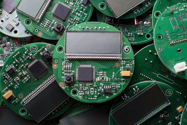
A round circuit board is commonly used when the PCB must fit inside a cylindrical enclosure, circular sensor, LED lamp, wearable device, motor housing or rotary control. Its electrical construction may resemble that of a rectangular PCB, but its mechanical manufacturing process requires different treatment. The main challenge is not drawing a circular outline. A round circuit board must remain stable while it passes through imaging, plating, solder-mask application, component assembly and depanelization. Incorrect contour data, weak panel support or poorly positioned breakaway tabs can damage the board edge and place stress on nearby components.
The Finished Diameter Begins With the Profile Data
PCB manufacturing data normally separates the electrical layers from the mechanical board profile. The circular outline should be supplied as one continuous closed contour with a clearly defined finished diameter. Duplicated lines, open arcs and overlapping segments can create uncertainty when the manufacturer prepares the routing program. A drawing that shows the diameter is useful, but it should not contradict the digital profile contained in the fabrication data. For a round circuit board, the center point and diameter also influence the locations of mounting holes, LEDs, switches and enclosure features. If the outline and component positions are created from different mechanical references, the finished PCB may be electrically correct but mechanically misaligned. Diameter tolerance should be based on the actual enclosure requirement. Specifying an unnecessarily tight tolerance increases manufacturing difficulty without improving product performance. Where the board fits inside a circular housing, the required radial clearance should account for both PCB-routing tolerance and enclosure variation.
Routing Creates the Circular Edge
Most circular PCB profiles are produced with a CNC router. A rotating cutting tool follows the programmed outline and removes the material around the finished board. The router diameter affects the space required between adjacent boards in a production panel. It also limits the smallest internal radius that can be produced in slots or notches. The manufacturer should therefore review any narrow mechanical feature connected to the circular outline. A round circuit board should not be represented as a filled circular image on a copper or solder-mask layer. The fabrication package needs a dedicated mechanical contour that distinguishes the finished external edge from internal slots and drilled holes. Routing direction, tool condition and feed rate affect the quality of the exposed laminate edge. A worn tool can leave rough glass fibers, resin smearing or dimensional variation. These problems become more noticeable on a circular profile because the tool remains engaged through a continuously changing direction.
Why Circular Boards Must Be Panelized
PCB factories do not normally process each small circular board separately. Multiple boards are placed inside a larger rectangular production panel so they can pass through standard fabrication and assembly equipment. The panel provides straight external edges for conveyor transport, tooling holes and fiducial marks. It also prevents individual boards from rotating or moving during solder-paste printing and component placement. Unlike a rectangular PCB, a round circuit board cannot normally be separated with straight V-scoring around its complete perimeter. Break routing is usually used instead. Most of the circular outline is routed in advance, while several small tabs keep the board connected to the surrounding panel frame. The location and quantity of these tabs determine whether the panel remains mechanically stable. Too few tabs allow the board to twist or vibrate. Excessively large tabs make separation difficult and can tear laminate from the finished edge. As one practical manufacturing reference, Eurocircuits recommends at least four breakaway tabs for round boards, with additional support for larger designs. The exact quantity, width and position should still be confirmed with the selected manufacturer because panel size, PCB thickness and assembly mass affect stability.
Tab Placement Affects More Than the Edge
Tabs should distribute support around the circumference rather than concentrating it on one side. Balanced placement reduces movement during solder-paste printing, component placement and reflow. However, a tab cannot be positioned solely according to geometric symmetry. Connectors, ceramic components, copper pours, antennas and mounting holes may require clearance from the separation area. When a round circuit board is broken out of the panel, force passes from the tab into the laminate. A nearby multilayer ceramic capacitor can crack even when the board itself appears undamaged. Solder joints near the edge may also experience bending stress. Mouse bites are sometimes added to breakaway tabs as a row of small holes that makes manual separation easier. They leave a rougher residual edge than fully routed removal, so they may be unsuitable when the circumference must slide into a close-fitting enclosure. For a smooth cosmetic edge, the manufacturer may remove the tabs with a routing or cutting process and then finish the remaining projections. The required edge quality should be stated before panel design because it influences both the tab method and secondary processing.
Copper and Components Need Edge Clearance
Copper placed too close to a routed outline can become exposed or damaged when the actual cut varies within manufacturing tolerance. The required setback depends on board class, layer registration, routing tolerance and whether exposed edge copper is intentionally specified. A round circuit board makes edge clearance more difficult to judge visually because traces, polygons and component pads approach a curved boundary at different angles. Automated design-rule checking should use the actual circular profile rather than an approximate square keep-out area. The edge-clearance review should include every copper layer, not only the visible outer layers. Internal power planes that extend too far toward the circumference can be exposed during routing even though the external artwork appears correct. Special structures require separate instructions. Castellated holes, plated edges and deliberate grounding contacts are not ordinary routing results. They need defined fabrication requirements and cannot be created safely by allowing standard copper to cross the cut line.
Assembly Equipment Still Needs Straight References
The PCB may be circular, but solder-paste printers and pick-and-place machines need stable tooling references. The surrounding panel frame provides these references while carrying fiducials and support holes. Panel fiducials should remain visible to the assembly equipment and should not be confused with circular copper features on the individual board. Local fiducials may also be useful around fine-pitch packages when the panel or board can experience dimensional variation. Component orientation deserves attention when heavy parts are placed near one side of a round circuit board. An unbalanced assembly can sag or rotate slightly if the breakout tabs do not provide sufficient support. This may affect solder-paste contact, component placement and conveyor handling. Tall edge connectors can also interfere with depanelization tooling after assembly. The panel layout must leave enough physical access to cut or route the tabs without contacting the connector body.
Depanelization Is a Controlled Manufacturing Step
Manual twisting is the simplest separation method, but it also produces the least controlled mechanical stress. Thin boards, ceramic components and solder joints located near the circumference are especially vulnerable. A fixture-supported cutter or depaneling router applies force more locally and provides a more consistent finished diameter. The correct method depends on volume, board thickness, edge-quality requirements and component placement. After separation, every round circuit board should be checked for laminate tearing, exposed glass fibers, copper exposure and excessive tab remnants. Dimensional inspection should measure the finished diameter after tab removal rather than measuring the routed section while the board is still attached to the panel. If the enclosure depends on a precise circular fit, inspection should also consider roundness. A board can meet the nominal diameter at one location while still having a local flat area or protruding tab residue that prevents installation.
Testing Must Include Mechanical Fit
Electrical testing confirms continuity and isolation, but it does not verify that the PCB fits the intended enclosure. A mechanical gauge or representative housing can identify contour and tab-removal problems before complete product assembly. For LED products, optical alignment may also depend on the relationship between the board center and the LED positions. Motor controls and rotary sensors can require similar concentricity between the PCB outline, center hole and sensing elements. A round circuit board should therefore be inspected as both an electrical circuit and a precision mechanical part. This is especially important when the outer edge is used to position the assembly inside the product.
When a Circular Shape Changes Cost
The circular outline itself does not necessarily make the bare PCB expensive. Cost rises when panel utilization is poor, wide spacing is required between boards, additional tabs are needed or the finished edge requires secondary machining. A round circuit board can leave unused areas between adjacent circular profiles in a rectangular manufacturing panel. Rotating or staggering the boards may improve material utilization, but the final arrangement must preserve routing access and panel stiffness. Cost is also influenced by whether the PCBs are delivered individually or kept in an assembly panel. Providing the manufacturer with expected order quantity, assembly method and edge-quality requirement allows the panel to be optimized before production. For round PCB projects entering fabrication and assembly, iPCB can review the mechanical profile, routing tolerance, panel arrangement, breakaway-tab positions and component-to-edge clearance before finalizing production data.
The Outline Must Be Treated as Part of the Product
A circular shape does not change the basic electrical function of a PCB, but it changes how the board is supported, routed, assembled and separated. The outline cannot be treated as a cosmetic feature added after the component layout is complete. A reliable round circuit board begins with unambiguous contour data and continues through stable panelization, controlled routing, suitable edge clearance and low-stress depanelization. When these steps are planned together, the finished board can retain its required diameter and edge quality without sacrificing assembly reliability.