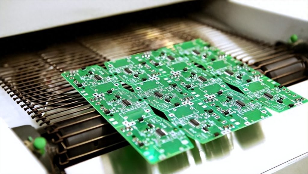
Splicing boards is the process of laying out multiple circuit boards on a single large size board to form an overall board assembly. The purpose of it is to maximize the use of board space, increase productivity and reduce costs.
Methods of splicing boards
1.V-CUT
V-CUT is to draw a slot in the connection of two boards, as long as the two boards together, leaving a little gap between them can be (generally 0.4mm), but the connection of the boards in this place is relatively thin, easy to break, and need to merge the edges of the two boards together when piecing.
V-CUT is generally a straight line, there will be no bending arcs and other complex alignment, try to spell the board in a straight line.
2.Stamp hole
For irregular PCB boards, such as round, V-CUT can not be done, this time you need to use to the stamp hole to connect the board, so the stamp hole is generally used in the shaped board more.
The edges of the two boards are connected by a small piece of plate, and this small piece of plate has many small holes in the connection with the two boards, so it is easy to break. After breaking, the edge of the board looks like the edge of a postage stamp, so this way of joining boards is called stamp holes.
3.Hollow connecting strip
Hollow connecting strip is used more in the circuit board with half hole process, is the use of very narrow plate for connection, and stamp holes are somewhat similar, the difference is that the connecting part of the strip is a little more narrow, and there is no hole on both sides.
There is one drawback to the hollow strip method of joining boards: when the boards are broken apart, there is a very noticeable bump. The stamp holes also have bumps, which are less noticeable because they are separated by the over-holes.
Some people might think that it would be better to just use the stamp holes, so why bother with the hollow connecting strips? This is because the stamp holes and the V-CUT cannot be used when the module is surrounded by half-holes, and can only be connected at the four corners of the module by hollow connecting strips.
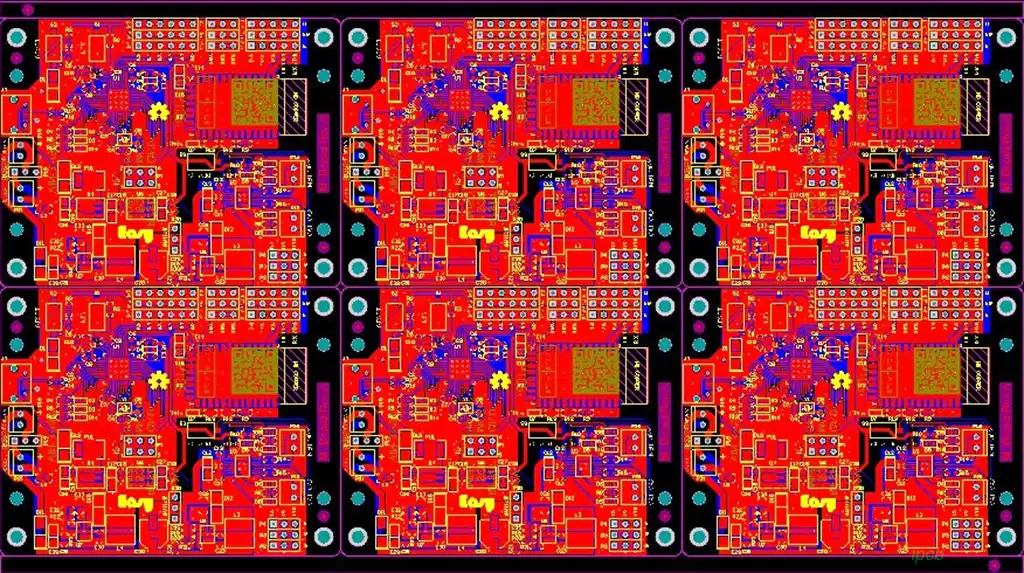
The purpose of piecing boards:
Improve productivity: In the PCB manufacturing process, splicing multiple individual boards into a whole board reduces the number of machine changeovers and adjustment time, and enables easier processing and assembly. For example, connectors for multiple small boards can be aligned more easily, which aids in subsequent testing and repair work.
Reduced costs: Reduces the cost of placing individual PCBs and improves the efficiency of the SMT machine’s placement head usage.
Reduce material waste: Reduce material loss due to placement failures.
Improve placement accuracy: Reduce cumulative errors in handling and positioning.
Optimize logistics and storage: Simplify handling and storage of large-size patch panels.
Reduce manual handling: Reduce the risk of manual errors and damage.
Increase automation: Adapt to automated production lines and increase the level of automation in the production process.
Convenient for testing and inspection: Inspect multiple PCB at the same time to quickly identify problems.
Environmentally friendly: Reduce material usage in the production process.
Adapt to different production needs: Adjust board size and shape according to order size and urgency.
Rules for assembling boards
- Try to put components of the same size and package together to minimize the gaps on the board.
- The spacing between components should be large enough to facilitate subsequent assembly and maintenance as well as to ensure electrical isolation between components.
- Strictly in accordance with the device design diagram of the board, to ensure that the electrical connections are correct, especially the power and ground connections must be accurate to avoid short circuits and other problems.
- Minimize the distance between components and metal edges to reduce electromagnetic interference between components and edges.
- Avoid crossing between components to reduce interference.
Putting together the board method
- Manual board piecing
Manual board is usually used for simple circuit boards, for larger, more dense components of the circuit board, manual board is less efficient and prone to errors. - Automatic board assembly
Automatic board assembly is usually carried out using machines, which can automatically and quickly put the components together, greatly improving work efficiency. The automatic board needs to write board rules to ensure the correctness and standardization of the board.
3.Mixed board
Hybrid PCB is a combination of manual and automatic PCB, which usually starts with automatic PCB by machine and then fine-tunes manually to ensure the accuracy and work efficiency of the board.
With the continuous development of the electronics industry, splicing boards technology has become an important means of improving production efficiency and reducing costs. Whether it’s V-CUT, stamp holes or hollow connecting strips, each type of board piecing has its own unique advantages and applicable scenarios.
