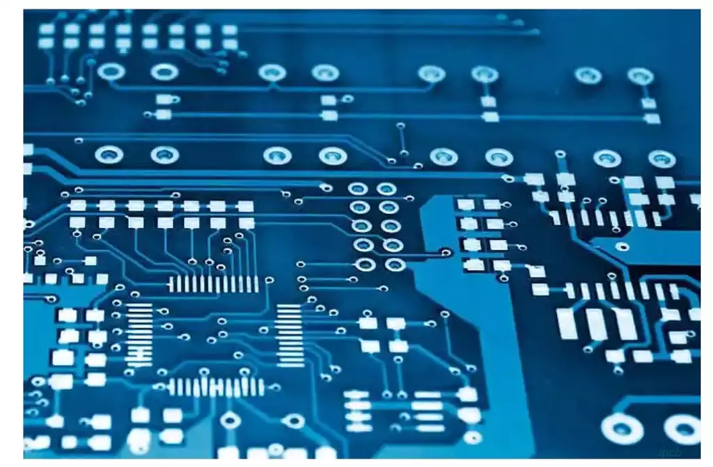
Exposed copper on pcb refers to the surface of the circuit board part of the copper foil is processed to remove the exposed place called exposed copper, also known as exposed copper over the holes, exposed copper heat dissipation, and so on. The PCB exposed copper is often used to strengthen the circuit board structure, improve the thermal performance of the circuit board, surface aesthetic treatment.
Reasons for exposed copper on PCB
- Design defects:
Improper design of soldermask: In the PCB design stage, inaccurate or negligent design of the soldermask leads to part of the copper surface not being effectively covered. (PCB circuit board soldermask usage)
Open area design: excessive open areas in the wiring design may lead to uneven distribution of plating current, affecting the uniformity of the copper layer.
- Process problems:
Improper etching and plating process control: improper etchant concentration, temperature control, or uneven plating current density may lead to copper layer defects.
Soldermask coating process problems: soldermask coating is uneven or not completely cover the copper surface, is a common cause of copper.
- Material factors:
Quality of substrates and copper foils: Selection of poor quality substrates or copper cladding foils will easily lead to poor adhesion of the copper layer and easy to fall off. (How to choose the right substrate according to the demand in PCBA processing?) - Use of the environment and external forces:
Temperature changes and mechanical stress: PCB in the process of use, by temperature changes or external mechanical stress, may lead to copper layer cracks or peeling.
Environmental factors: high humidity environment can easily lead to PCB board moisture, accelerate the oxidation of copper layer.
Hazards of exposed copper on pcb
Electrical performance degradation
Exposed copper in the area of the copper foil in direct contact with the air, it is very easy to oxidise, the formation of poor conductivity of the copper oxide layer, resulting in increased line resistance, signal transmission instability. If copper exposure occurs on high frequency signal lines, it will also cause signal attenuation and interference, seriously affecting the communication and computing performance of the equipment.
Increased risk of short-circuit
A short-circuit fault may be triggered when the exposed copper area comes into contact with adjacent lines or grounding layers, or when metallic debris or conductive liquid adheres to it. In power supply circuits, short circuits can lead to component burnout and even serious accidents such as fires.
Shortened service life
Oxidised copper foil will continue to corrode, causing the lines to gradually thin and break, which can lead to functional failure of the circuit board. Even if there is no short-circuit, exposed copper will accelerate the aging process of the circuit board, shortening the overall service life of electronic equipment.
Copper exposure is a common problem in PCB manufacturing, affecting the electrical performance, reliability and overall quality of the board. The following are for different degrees of copper treatment:
Board copper treatment
Mild copper treatment
Soldermask repair
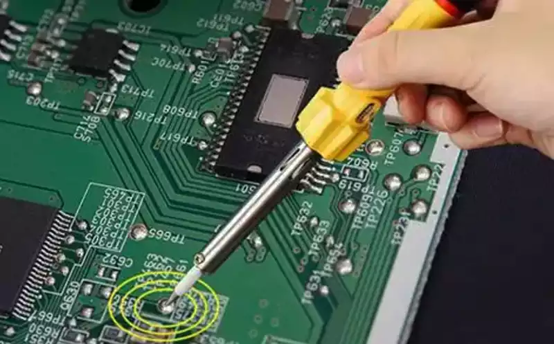
For a small area and the location of the copper is not critical to the exposed area, you can use a special soldermask to repair. First of all, you need to clean the exposed copper surface, remove the oxide layer and impurities. Then, apply the solder resist evenly to the exposed copper and allow it to dry and cure to re-form the protective insulation layer. When doing so, care should be taken to ensure that the thickness of the application is uniform to avoid the creation of new air bubbles or thickness deviations.
Applying insulating varnish
If a solder resist pen is not available, insulating varnish is also an option for repair. The insulating varnish has good electrical insulation properties and adhesion, and can effectively isolate the air from the copper foil. It is recommended to use a fine-bristle brush to ensure a thin and even layer of paint. Check the insulation effect after drying and repeat the application if necessary.
Moderate Copper Exposure Treatment
Local Mount Insulation Tape
For slightly larger and more complex location of copper exposure area, high temperature resistant and good insulation properties of polyimide tape can be used to cover. The exposed copper surface should be cleaned before operation, and then cut the tape to the right size to precisely cover the exposed copper area, and make sure that the edge of the tape is tightly adhered to the board to prevent water vapour and contaminants from seeping in.
Reprinting Soldermask
When there are multiple exposed copper surfaces on the pcb board or the exposed copper areas have high insulation requirements, the method of reprinting the soldermask can be used. This method requires specialised equipment and processes and usually involves sending the board back to the manufacturer or a specialist repair facility for processing. The repairer will first clean and pre-treat the circuit board, and then re-apply the soldermask through the processes of screen printing, exposure and development. In addition, the amount of ink used in screen printing can be increased by increasing the thickness of the water film, thus improving the ability of the ink to cover the surface of the vias and effectively avoiding the phenomenon of false copper exposure.
Other Production Control Methods
In the PCB manufacturing process, in order to avoid pcb exposed copper, you can strictly control the process parameters of etching, plating, soldermask coating, etc., and ensure that the operation is standardised. For example, in the screen printing step, you can set the screen printing pressure of 6Kg/cm2, screen printing speed of 2m/min, and the viscosity of 150dpa.s solder resist ink. In the baking step, the temperature can be controlled at 150℃-160℃ and the baking time is 90min-150min to ensure that the solder resist ink is permanently cured. For copper exposure that has occurred, a selective plating process can also be used to deposit other metals on the exposed copper to enhance protection. For pseudo-coppering, a processing method includes cleaning, multiple screen printing, multiple pre-baking, alignment, exposure, developing and baking steps. The cleaning step may include pickling with 3% sulfuric acid and diamond grinding to remove oxides, corrosion and burrs.
PCB exposed copper solutions
- Optimisation at the design stage: Ensure that the design of soldermask is accurate, avoid the design of open areas, and try to spread copper to balance the plating current. Communicate fully with the customer to clarify the details of the processing requirements such as holes, to avoid false pcb exposured copper.
- Production control: Strictly control the process parameters of etching, plating, soldermask coating, etc. to ensure that the operation is standardised. Adopt high-precision equipment and professional operation skills to ensure that the solder resist layer evenly covers the copper surface. For specific processes such as plugging holes in aluminium sheets, it is necessary to adjust the degree of alignment, squeegee pressure and angle to ensure that the ink enters the holes completely.
- Local repair: For PCBs with exposed copper, special soldermask or repair adhesive can be used for local repair to form an insulating protective layer. Under certain circumstances, selective plating process can be used in the exposed copper deposited on other metals to enhance the protection.
- Environmental control and protection: In the process of PCB use, pay attention to environmental humidity and temperature changes, take appropriate protective measures. Enhance the mechanical strength of the PCB design, to avoid external stress caused by the copper layer off.
Exposed copper on pcb is a complex problem caused by various factors, in order to ensure the long-term stable operation of the circuit board and the performance of the equipment, must be in the PCB design, manufacturing and post maintenance, comprehensive consideration and take effective preventive and repair measures. Through continuous optimisation of the design, strict control of the production process, the use of high-quality materials, and pay attention to the protection of the use of the environment, you can minimise the occurrence of the copper phenomenon, so as to enhance the reliability, durability and overall performance of the circuit board.