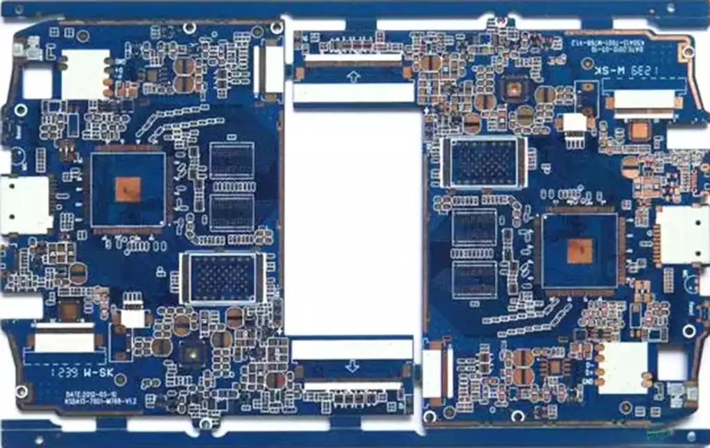
The laminate design of FPC antennas is fundamentally an engineering solution aimed at ensuring effective signal transmission. It comprises multiple layers of materials with distinct functions, each requiring a delicate balance of electrical performance, mechanical strength, manufacturing feasibility, and cost control.
Design rationale and key process parameters for each functional layer
Surface protective layer
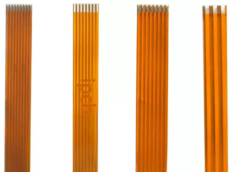
Serving as the fpc antenna‘s outer cladding, the surface protective layer must withstand external environmental corrosion without compromising the antenna’s inherent flexibility. In consumer electronics, polyimide (PI) film remains the predominant choice, with its mature manufacturing processes and stable performance being key considerations.
Material Selection Logic: PI’s widespread adoption stems from its balanced performance profile—its temperature tolerance (-40°C to 125°C) covers standard consumer electronics operating conditions; its flex endurance (typically exceeding 100,000 cycles) withstands daily use; coupled with a mature PI supply chain and controllable costs, it serves as a universal solution.
Thickness Control: Within consumer electronics, the thickness window typically ranges from 0.02mm to 0.05mm. Below 0.02mm, damage rates during production and processing increase significantly; above 0.05mm, it directly compromises the product’s overall slimline objectives, while excessively thick protective layers may introduce non-negligible dielectric loading effects on high-frequency signals. In demanding environments like automotive applications, thicker (0.05mm–0.08mm) high-performance PI or modified PTFE is employed to meet higher weather resistance and impact rating requirements.
Signal Circuit Layer
The signal circuit layer constitutes the antenna’s core. Its pattern precision and material directly determine whether the antenna operates within the target frequency band and efficiently radiates signals.
Copper Foil Selection: Electrolytic copper foil is extensively used in standard consumer electronics due to its cost advantage and stable conductivity (approximately 97%–98% IACS). Rolled copper foil, though slightly more expensive, offers superior ductility and fatigue resistance, making it essential for dynamic bending applications in foldable devices and smart wearables. While both foils exhibit comparable electrical conductivity, their primary distinction lies in mechanical stress tolerance.
Design Parameter Implementation: Trace width and spacing are not isolated design elements but require comprehensive simulation considering antenna configuration, frequency band, and laminate structure. Taking 5G smartphones as an example: high-frequency bands are sensitive to loss, necessitating line widths of 0.1mm–0.2mm and spacings no less than 0.1mm to suppress coupling interference and maintain gain within limited clearance. Conversely, low-frequency bands permit wider line widths (0.2mm–0.3mm) to reduce etching complexity and enhance yield.
Routing Principles: Signal paths adhere to the shortest-path principle to minimise conductor loss. When single-layer routing cannot accommodate multi-band or complex feed requirements, dual-layer or multi-layer circuit designs are employed. Interconnections are achieved through precise interlayer vias, imposing stringent demands on subsequent interlayer alignment accuracy.
Insulating Medium Layer
Situated between the circuit layer and ground plane, the material selection and thickness of this layer directly influence signal loss and laminate reliability.
Material Selection: Polyimide (PI) film remains the primary insulating material for mid-to-high-end FPC antennas. Its high breakdown voltage (≥100kV/mm) and excellent thermal resistance ensure reliability during processing and operation. Polyethylene terephthalate (PET) film, leveraging its cost advantage, retains a niche in entry-level products with shorter lifecycles and less stringent performance requirements.
Thickness Matching: Thickness design must be strongly correlated with the operating frequency band. At high frequencies, to minimise dielectric loss, the insulating layer thickness must be strictly controlled to be thin (0.03mm–0.06mm); for low-frequency applications, it can be appropriately increased (0.06mm–0.1mm) to enhance electrical isolation and stacking rigidity.
Process Control Points: During production, the coating flatness of the insulating layer is a core control item. Any bubbles, impurities, or thickness irregularities (typically tolerated at ≤±0.005mm) may initiate subsequent bending fractures or cause impedance discontinuities. Consequently, precision coating and in-line thickness scanning are standardised processes.
Ground plane
The ground plane provides a reference ground and return path for signals while also serving as a shield, being crucial to the antenna’s interference resistance.
Material and Thickness: The material matches that of the signal layer (copper foil). To achieve lower DC resistance and better shielding continuity, its thickness is typically slightly greater than the signal layer, generally ranging from 0.05mm to 0.1mm. The core design principle is ‘complete coverage wherever possible’, avoiding narrow gaps or isolated islands. Particularly at high frequencies, the integrity of the ground plane directly determines the antenna’s radiation efficiency and immunity to interference.
Design Flexibility: Ground plane requirements vary by antenna type. For instance, PIFA antennas demand tightly coupled ground, while certain dipole antennas necessitate carefully engineered ground dimensions and shapes to shape radiation patterns. In products operating within complex electromagnetic environments like automotive applications, the ground plane incorporates multiple interfaces connected to system ground points to ensure stable ground potential during operation.

Functional Auxiliary Layers
Shielding Layer: Not required for all FPC antennas. Only in high-EMI environments like automotive or industrial control systems is an additional metal layer (copper foil, aluminium foil, or coating) incorporated into the stack-up. This layer, typically 0.02mm to 0.05mm thick, must be reliably connected to the main ground plane at multiple points to create a Faraday cage effect.
Bonding Layer: This acts as the adhesive bonding different layers together, being extremely thin (0.01mm–0.03mm) yet critically important. The manufacturing challenge lies in achieving uniform coating thickness—avoiding both adhesive shortages that cause delamination and excess adhesive that contaminates traces or blocks vias. The lamination temperature (170°C–190°C) and pressure (20 kg/cm²–30 kg/cm²) curves must be precisely calibrated according to the material system.
Reinforcement Layer: This addresses localised rigidity requirements in flexible boards. At points needing support—such as insertion interfaces and solder terminals—local reinforcement is achieved using FR-4 rigid boards or thickened PI. Thickness varies from 0.2mm to 0.5mm depending on stress conditions, serving as a standard method to ensure assembly reliability.
Four Core Processes Determining Laminate Quality
Interlayer Registration: For multilayer boards, interlayer registration accuracy is the lifeline of yield. Industry standards mandate tolerances within ±15μm, achieved through CCD optical registration systems and stable thermal expansion control. Inaccurate registration causes impedance deviations at best, and interlayer shorts or breaks at worst.
Etching Precision: Circuit pattern integrity directly impacts antenna performance. Precision etching requires strict control of chemical concentration (e.g., 100g/L to 120g/L), temperature (45°C to 55°C), and conveyor speed. This ensures line width tolerance remains within ±0.01mm, with clean edges free of burrs. It prevents insufficient line width from over-etching or short circuits from under-etching.
Lamination reliability: The lamination process aims to eliminate interlayer voids and ensure complete adhesion. Parameters such as temperature, pressure, and dwell time must be adjusted according to substrate material (PI or PET). Post-lamination cooling rates (e.g., 5°C/min to 10°C/min) require precise control to release internal stresses, preventing warping or delamination during subsequent processing or use.
Comprehensive inspection: Finished products must pass multiple stages: visual inspection (free from scratches, indentations, delamination, contamination), dimensional measurement (within permissible tolerances), electrical testing (S-parameter measurement via network analyser, ground continuity, insulation resistance), and necessary mechanical property sampling (bend testing, solder resistance). Only after passing this series of verifications is the product truly ready for delivery.
It is precisely this deep integration of materials science and precision engineering that enables FPC antennas to achieve efficient signal transmission within their compact dimensions. The functional trade-offs and parameter control across each layer ultimately converge towards a single objective: providing a stable and reliable physical foundation for wireless communication within complex application environments.