FPC antennas, formally known as flexible printed circuit antennas, are specialised antennas that integrate key functional components such as the antenna radiation unit and feed structure onto a flexible PCB substrate.
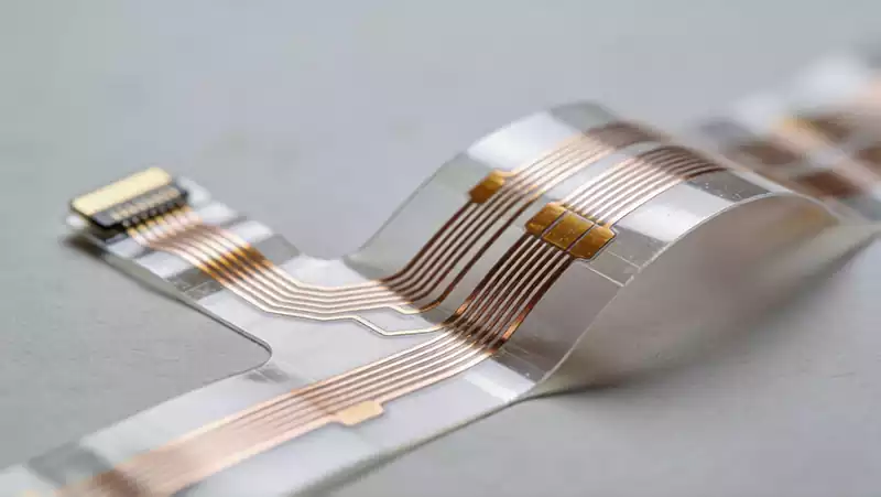
The FPC antenna comprises key components including a flexible substrate, radiating elements, feed points, ground planes, and coaxial cables. The flexible substrate serves as the physical carrier for the FPC antenna and underpins its inherent flexibility. Commonly employed materials are polyimide (PI) or liquid crystal polymer (LCP), with thicknesses ranging from 0.1 to 0.2 millimetres, achieving weight reductions exceeding 50% compared to traditional metallic antennas.
This material not only exhibits outstanding flexibility and fold resistance, maintaining the integrity of its conductive structure when bent or folded, but also possesses excellent electrical insulation and high-temperature resistance, enabling adaptation to complex and variable internal device environments. The manufacturing precision of the substrate is directly determined by the cutting and surface treatment stages within the PCB process. Its flatness and insulation properties critically influence the subsequent conductive efficiency of the radiating elements and the final signal quality.
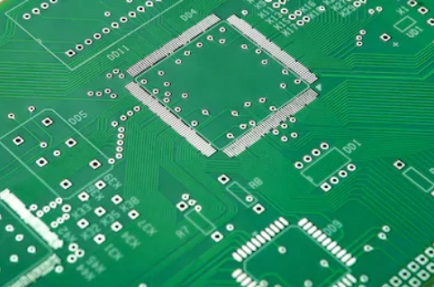
As the ‘signal core’ of FPC antennas, radiating elements undertake signal transmission and reception functions. Typically formed by copper foil through PCB etching processes and laid upon the substrate surface, their shape, dimensions, and layout directly determine the antenna’s operating frequency bands and signal strength. Common structures include rectangular, circular, and folded-line configurations to accommodate different resonant frequencies.
For instance, FPC antennas designed for 5G or WiFi often employ specific zigzag structures in their radiating elements to cover high-frequency bands like 2.4GHz and 5GHz. Manufacturing precision for this component demands micrometre-level etching accuracy; dimensional deviations would otherwise cause electromagnetic resonance to deviate from design targets, leading to signal stuttering or reduced transmission range.
The feed point acts as a ‘signal relay station’, facilitating RF signal transfer between the main board and radiating elements. Typically positioned near the centre of the radiating element’s ground plane, it establishes electrical connectivity to the main board via soldering. Contact stability is paramount, with soldering quality and pad design during PCB manufacturing directly impacting conductivity. Inadequate soldering or suboptimal pad structure causes signal loss and poor contact, thereby diminishing the antenna’s overall efficiency.
The ground plane functions as a ‘signal stabiliser,’ typically constructed from copper foil. It may be positioned on the same or opposite side of the flexible substrate, maintaining a specific distance from the radiating element. Its role is to suppress external electromagnetic interference, enhance signal stability, and simultaneously form electromagnetic coupling with the radiating element to amplify resonance effects.
In design, the spacing between these two elements is typically controlled within 1 millimetre, with their centrelines aligned to maximise interference resistance. Ground plane dimensions also require strict control; for instance, the length of a WiFi antenna’s ground plane along the centreline is usually 13.5±0.05 millimetres, and 17.5±0.05 millimetres in the perpendicular direction. Such precision relies on the support of PCB manufacturing processes.
Beyond the four core components, coaxial cable serves as a vital auxiliary structure within FPC antennas. Comprising a core wire, dielectric layer, shielding layer, and protective layer, it connects the feed point to the core wire and the ground plane to the shielding layer. This configuration facilitates signal transmission while further isolating external interference and minimising signal loss. Manufacturing quality—including the precision of shielding layer wrapping and the conductivity of the core wire—directly impacts transmission performance.
The Entire Operational Process of FPC Antennas
Their core operating principle lies in achieving the reception and transmission of radio frequency signals through the electromagnetic coupling and resonance mechanisms of conductive structures—converting external electromagnetic waves into electrical signals processable by the device, or transforming internal electrical signals into electromagnetic waves for radiation. Compared to traditional rigid PCB antennas, FPC antennas leverage the flexibility, bendability, and slim profile of their flexible substrates to adapt seamlessly to diverse complex installation environments. This performance advantage stems not only from their unique structural design but also from high-precision PCB manufacturing processes. FPC antennas achieve efficient conversion between electrical signals and electromagnetic waves through ‘resonance’, encompassing both signal reception and transmission phases.
During signal reception, external electromagnetic waves act upon the radiation unit, inducing currents within it that are converted into electrical signals. In this process, the ground plane serves to isolate the device from internal electromagnetic interference while forming electromagnetic coupling with the radiation unit, thereby enhancing signal strength. Subsequently, the induced electrical signals are transmitted via the feed point to the mainboard’s RF module, where they undergo amplification and demodulation before being converted into digital signals recognisable by the device.
During signal transmission, the radio-frequency electrical signal generated by the device’s mainboard is transmitted via the feed point to the radiation unit. An alternating current is formed within the radiation unit, exciting an alternating electromagnetic field that radiates energy outward in the form of electromagnetic waves. At this stage, the ground plane effectively suppresses electromagnetic wave leakage into the device’s interior, safeguarding the normal operation of other components. Simultaneously, it optimises the resonance effect of the radiation unit, enhancing transmission efficiency.
The core principle of this process is the ‘resonance’ mechanism, wherein the resonant frequency of the radiating element must align precisely with the RF signal frequency. Achieving this state relies on the precise control of the radiating element’s shape, dimensions, material, and ground plane layout. These parameters are all ensured through the PCB manufacturing process. Similarly, bending or folding during FPC antenna installation alters the structural form of the radiating element, thereby affecting its natural frequency. Consequently, the flex substrate’s resistance to bending and folding becomes a critical factor in ensuring stable antenna performance.
The production of FPC antennas involves multiple key processes, with each stage collectively determining the antenna’s final performance and reliability.
Substrate preparation forms the foundational stage of production. Cleaning, polishing, and surface activation of the flexible substrate (PI or LCP) remove impurities and contaminants, enhancing adhesion between the substrate and copper foil. Inadequate processing may lead to subsequent copper foil delamination or peeling, compromising conductivity and increasing signal loss. Concurrently, substrate thickness and flatness require stringent control. For instance, LCP substrates exhibit exceptionally low dielectric loss (tanδ) of 0.002–0.005, significantly outperforming traditional PI materials. This makes them particularly suitable for high-frequency signal transmission, such as 5G millimetre-wave applications. However, realising this performance hinges on the precision of substrate selection and processing techniques.
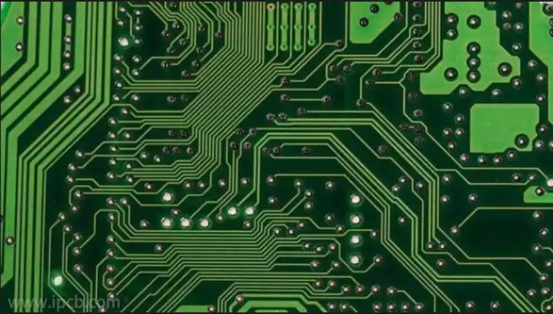
The etching process constitutes the core manufacturing stage, precisely shaping the copper foil into the required structures—such as radiating elements and ground planes—as specified in the design. This process employs photolithography to transfer patterns onto the copper foil surface, followed by chemical etching to remove excess material. Etching tolerances must be maintained within ±0.05mm; deviations beyond this range cause dimensional inaccuracies that compromise resonance performance and signal integrity. Radiating elements, for instance, typically require length and width tolerances within this precision range, achievable only through high-accuracy etching.
The soldering process establishes electrical connections between feed points and coaxial cables or device motherboards, with its quality directly impacting signal transmission stability. Precision soldering techniques must be employed during manufacturing to ensure robust connections between feed points and core wires, as well as between ground planes and shielding layers, minimising contact resistance and preventing issues such as cold solder joints or false soldering. Simultaneously, soldering temperature and duration require strict control to prevent high-temperature damage to the substrate or conductive structures.
The lamination process serves as a protective measure prior to final assembly. By applying a layer of polyimide or polyester film over the conductive structures, it provides insulation, moisture resistance, and abrasion protection, thereby extending the antenna’s service life. The film thickness must balance protective efficacy with flexibility, and the film layer must adhere tightly to the conductive structures without bubbles or wrinkles to prevent structural damage from delamination.
Prior to shipment, FPC antennas undergo a series of performance tests, including signal strength, resonance frequency, bend resistance, and high-temperature endurance, to ensure compliance with diverse application requirements. For instance, automotive antennas must pass high-temperature and vibration tests to guarantee stability during vehicle operation, while smart wearable antennas endure repeated bending tests to ensure uninterrupted signal transmission during prolonged wear.
The performance of FPC antennas hinges critically on the synergy between material properties and manufacturing precision. From substrate preparation to precision etching, and from stable soldering to reliable coating application, each process step directly influences signal transmission quality and antenna operational stability. Consequently, amid trends towards higher frequencies and miniaturisation, the continuous refinement of PCB manufacturing techniques remains pivotal to enabling FPC antennas to adapt to increasingly complex application scenarios.