HDI Flex PCB is efficient and reliable circuit board with multiple electronic components. They offer better electrical performance in a smaller package size due to the use of thin, non-conductive substrate materials. HDI flex pcb primarily made from flexible substrates such as polyimide, which are lightweight and easily bendable to accommodate devices with complex shapes. Due to its flexibility, hdi flex pcb is widely used in consumer electronics, medical devices, aerospace, automotive electronics and other industries, especially in space-limited application scenarios, which can effectively reduce the volume and weight of products.
HDI flex pcb has several significant advantages over traditional circuit boards:
enables more complex circuit layouts, and its high-density interconnect technology allows circuits to be more compact and reduces the distance between components, thus improving circuit integration. This is particularly important for the ever-shrinking size requirements of modern electronics.
With good flexibility, they can be adapted to complex three-dimensional structural designs in a limited space. For example, they can be bent, folded, and even curled, making them widely used in areas such as wearables, smartphones, and medical devices.
With their lighter weight, they can significantly reduce the overall weight of a product compared to traditional circuit boards. This not only helps to improve the portability of the product, but also helps to reduce transport costs.
HDI Flex PCB Manufacturing Process
Design and Layout
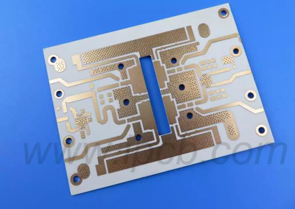
The manufacturing process starts with a fine circuit design, using advanced EDA software for precise layout, and reasonable planning of the stacked layer structure, via hole types and component arrangement. Special emphasis is placed on the design of blind, buried and microvias to achieve high interconnect density.
Material Selection and Preparation
Flexible polymer substrates such as polyimide are used, while compatible dielectric materials and copper foils are selected to ensure good adhesion between materials and stable electrical properties. The glass transition temperature (Tg), thermal shock tolerance and dielectric spacing of the materials need to meet manufacturing and reliability requirements.
Stack Building and Lamination
Sequential lamination technology is applied to precisely laminate multiple layers of flexible substrates and copper layers to form a multilayer circuit structure. The process requires tight control of temperature, pressure and time to ensure a strong bond between layers and no voids.
Microvia Formation and Metallisation
Microvias are formed by laser drilling with extremely small hole diameters (generally less than 0.15 mm), followed by chemical copper immersion and plating to complete the metallisation of the microvias and to ensure electrical connectivity between the layers. The process control requirements are high, otherwise it is easy to produce hole wall cracks or copper skin peeling.
Cabling Etching and Line Fabrication
Utilises high precision etching processes and automated alignment equipment to achieve fine line width and fine pitch line pattern fabrication to ensure signal integrity and impedance control.
Testing and Assembly Preparation
After completing the signal lines and interconnect structures, quality assurance is provided for subsequent assembly and final application through various electrical and mechanical performance tests, such as impedance tests and bending tests.
Reliability testing of hdi flex pcb is a critical step to ensure their stable operation in actual use. Common reliability tests include:
Thermal cycling test: The circuit board is placed in different temperature environments and repeatedly heated and cooled to detect whether the material will produce micro-cracks or undergo deformation under temperature fluctuations.
Humidity test: examine the humidity resistance of the circuit board under high temperature and high humidity conditions, observe the changes in its insulation properties and mechanical strength, and ensure that it is still reliable in a humid environment.
Mechanical shock test: simulate the actual use or transport process may encounter shock and vibration, assess the impact resistance of the circuit board to ensure that it is not easy to damage.
Tensile Test: Tensile testing of flexible pcb boards to check their tensile strength and ductility to ensure that they will not break under bending or stretching.
Electrical performance test: including DC resistance, insulation resistance and dielectric properties of the test, to ensure that the circuit board in the operation of the electrical properties of stable and good.
Soldering Reliability Tests: such as hot air reflow soldering tests, are used to assess the robustness of the solder joints and ensure that the boards still meet the requirements for connectivity after soldering at high temperatures.
HDI flex pcb application areas:
In the consumer electronics industry,hdi flex pcb is widely used in products such as smartphones, tablets and wearable devices. These devices have strict restrictions on the size and weight, hdi flex pcb can achieve high performance interconnections in a limited space to meet the needs of thin and light design.
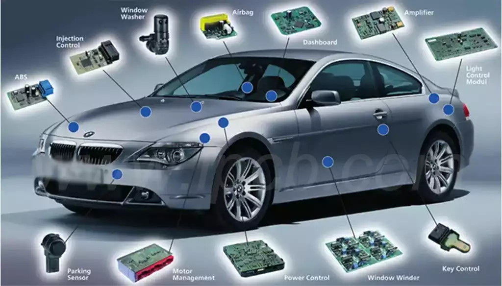
In the field of automotive electronics, with the development of smart cars and assisted driving technology, hdi flex pcb is gradually becoming key components. It can flexibly adapt to complex space wiring, support a variety of sensors and control units, and enhance the level of vehicle intelligence and safety performance.
In the field of medical equipment, hdi flex pcb is used in portable medical instruments and implantable devices. These circuit boards are compact in size, have good biocompatibility, and can work stably and reliably in complex biological environments.
As the performance and reliability of electronic products continue to improve, hdi flex pcb, as the core component of high-density interconnect and flexible design, the manufacturing process and strict testing standards have become particularly important. Advanced design layouts, high-precision manufacturing processes, and comprehensive reliability testing can ensure that it continue to maintain excellent electrical and mechanical properties in complex environments. In the future, with the continuous progress of material science and manufacturing technology, the quality and application scope of hdi flex pcb will continue to improve, providing a solid guarantee for the realisation of intelligent, high-performance electronic products.