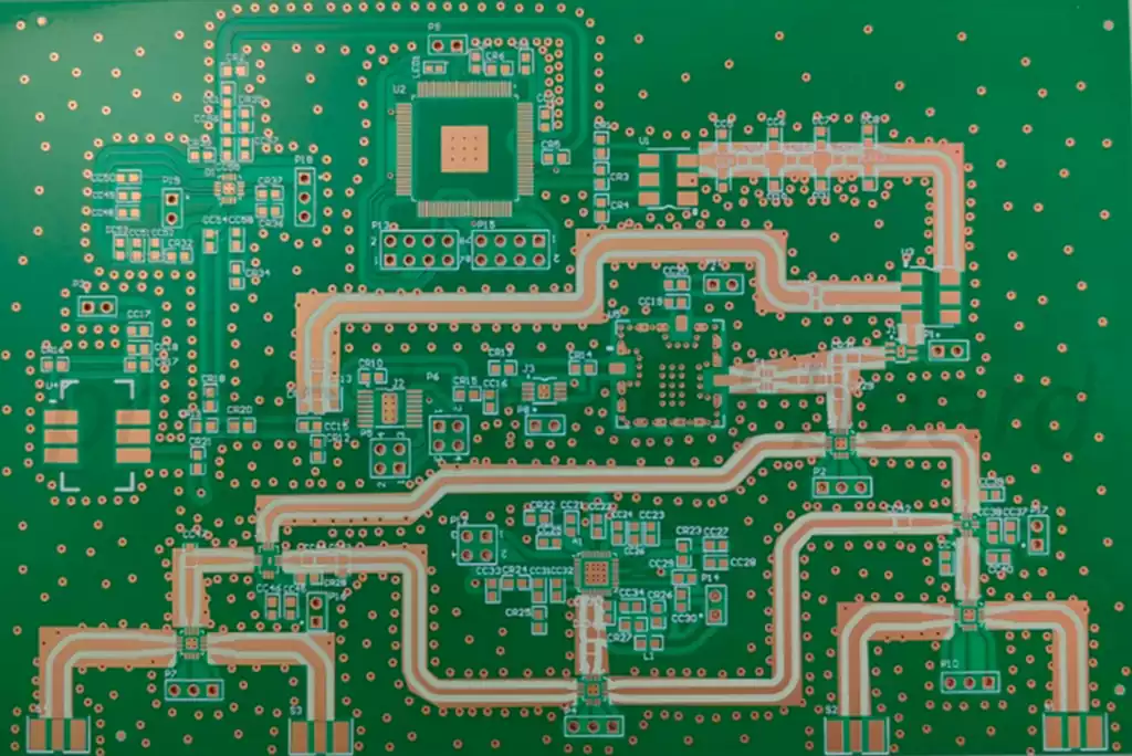
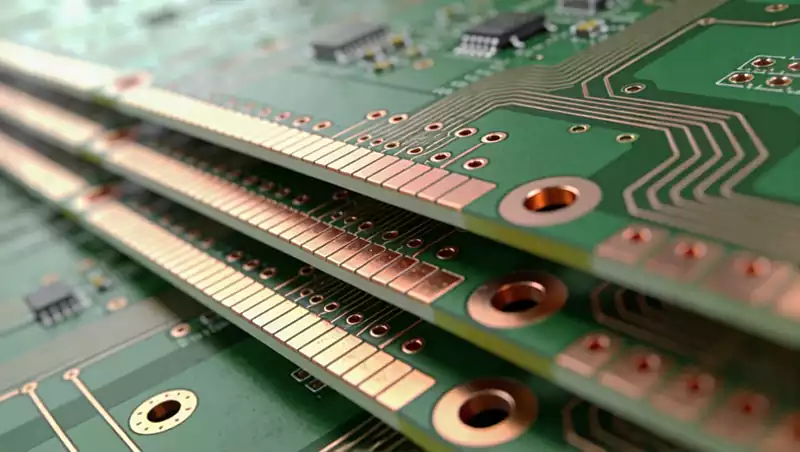
The complex processes involved in HDI PCB, such as laser microvia drilling and multi-layer buried/blind vias, while enhancing interconnect density, also exponentially increase the risk of manufacturing defects. A mere 0.075mm deviation in a microvia or a micrometre-level flaw in the copper plating can lead to signal attenuation, continuity failure, or even cause end-device malfunctions. Accurate identification of high-frequency defects and mastery of core mitigation methods are not only pivotal to ensuring HDI PCB mass production yield rates, but also fundamental prerequisites for controlling manufacturing costs and enhancing product reliability. Furthermore, they form the foundational support for the stable deployment of high-end electronic equipment.
1.Laser Microvia Defects
As a core HDI PCB process, laser microvia precision directly determines product performance. Common defects manifest as excessive ablation, rough via walls, or microvia blockage, often stemming from parameter settings, substrate characteristics, and equipment conditions.
Excessive ablation frequently results from overly high laser energy or excessively slow processing speeds, causing carbonisation of the substrate around the microvia and deformation of the pad. In severe cases, this can compromise the interlayer insulation structure, leading to signal crosstalk. Such defects pose significant hazards in high-frequency applications, increasing insertion loss by over 3dB for signals above 5GHz and potentially causing complete circuit failure. Mitigation hinges on precisely matching laser parameters to substrate properties: for FR-4 substrates, controlling laser energy between 8-12μJ and maintaining processing speeds at 3000-5000 holes per minute, while employing pulsed lasers over continuous ones to reduce heat accumulation. Pre-baking substrates prior to processing to remove internal moisture further lowers carbonisation probability. A certain automotive HDI PCB manufacturer reduced ablation defect rates from 4.2% to 0.8% through parameter optimisation.
Via wall roughness and micro-via blockage are closely linked to consumable quality and processing environment. Via wall roughness, caused by laser focus deviation and uneven filler distribution in the substrate, compromises copper plating adhesion, potentially leading to peeling during subsequent use. Micro-via blockages frequently result from inadequate debris removal or resin overflow, particularly prevalent in resin-filled Via-in-Pad processes. Dual-pronged control measures are essential: equipment-side requires regular calibration of laser focusing lenses to ensure spot accuracy; process-side necessitates optimised dust extraction systems employing combined high-pressure air blowing and vacuum suction for debris clearance. Post-resin filling, incorporate secondary polishing to guarantee unobstructed micro-via conductivity.
2.Buried Blind Via Interconnection Defects
The interlayer alignment precision and electrical continuity stability of buried blind vias represent another core challenge in HDI PCB manufacturing. Common defects include misalignment, via wall voids, and incomplete via penetration. These defects are highly concealed, requiring specialised equipment for detection, and present extreme difficulty in rectification.
Alignment deviation represents the most typical buried/blind via defect, often stemming from inaccurate inner-layer pattern positioning or substrate shrinkage during lamination. Deviations exceeding 0.1mm directly result in insufficient contact area between the via wall and pad, causing conductance resistance to surge dramatically. Particularly in second-order and higher HDI PCBs, nested multi-layer buried/blind via designs compound alignment errors, leading to an exponential increase in defect risk. Mitigation requires source control: employ high-precision locating pins and optical alignment systems to confine inner layer pattern positioning errors within 0.02mm. Pre-stretch substrates prior to lamination to match thermal expansion coefficients of different layer materials, minimising lamination deformation. Concurrently, optimise panelisation designs to prevent alignment deviations caused by uneven stress distribution at panel edges.
Hollowed-out hole walls and non-through buried holes stem from improper electroplating processes and drilling parameters. Hollowed-out walls occur when copper plating fails to fully cover the hole wall during electroplating, creating localised voids prone to fracture during thermal cycling. Non-through buried holes are primarily caused by inadequate drilling depth settings or insufficient cutting force due to drill bit wear. Control strategies include: optimising electroplating parameters by employing pulse plating technology to enhance copper deposition uniformity, ensuring hole wall copper thickness meets specifications (≥18μm); regularly replacing drill bits; adjusting drilling speed and feed rate according to substrate type; maintaining buried hole depth tolerance within ±0.05mm; Post-plating X-ray inspection (AXI) to detect bore wall defects and promptly reject non-conforming parts.
3.Copper Plating and Surface Treatment Defects
The copper plating layer and surface treatment processes of HDI PCB directly impact the product’s electrical continuity stability and corrosion resistance. Common defects include uneven copper plating thickness, residual copper particles, and surface treatment layer delamination. Such defects are prone to causing failures during the later stages of product use and are difficult to trace.
Uneven copper thickness predominantly occurs in microvias and buried/blind vias, stemming from uneven current distribution and imbalanced plating solution concentrations. Thick copper areas may suffer from inadequate heat dissipation, while thin copper regions exhibit excessive contact resistance, impairing signal transmission and current-carrying capacity. Mitigation requires optimising plating bath formulations by adding levelling agents and brighteners to ensure uniform solution distribution. Employing pictorial anodes tailored to HDI PCB complexities maintains consistent current density (1-2 A/dm²) across microvias and surface areas. Regular monitoring of bath concentration and temperature prevents parameter fluctuations causing plating irregularities.
Copper particle residue and surface treatment layer delamination relate to process cleanliness and workflow control. Residual particles typically stem from inadequate post-plating rinsing, where minute copper debris adheres to the board surface, potentially causing short circuits. Surface treatment layer delamination (e.g., ENIG, electroless nickel immersion silver) arises from insufficient board cleaning or excessive processing temperatures, resulting in poor adhesion between the coating and substrate. Control measures require enhanced cleaning procedures across all stages. Employ a combination of ultrasonic cleaning followed by high-pressure water rinsing post-plating to remove residual copper particles and impurities. Optimise surface treatment parameters: maintain ENIG process temperatures between 85-90°C and control electroless nickel plating duration at 60-90 seconds. Conduct tape tests post-treatment to verify coating adhesion and ensure no delamination occurs.
4.Material and Laminating Defects
HDI PCB demands exceptionally high material performance and lamination process standards. Substrate defects, lamination bubbles, and uncontrolled resin flow fundamentally compromise product structural integrity, often leading to widespread defects during mass production.
Substrate defects typically stem from inadequate procurement controls, where sheets exhibit pinholes, impurities, or thickness inconsistencies. These issues readily cause micro-cracking and interlayer delamination during subsequent processing. Mitigation requires stringent incoming material inspection, employing optical detection equipment to screen for substrate pinholes and impurities, with thickness tolerances controlled within ±0.01mm. Prioritise high-purity substrates specifically formulated for HDI processes to prevent processing defects caused by uneven filler distribution.
Pressure bonding bubbles and uncontrolled resin flow represent core challenges in the bonding process. Bonding bubbles arise from residual moisture in substrates and suboptimal temperature-pressure curves during bonding, compromising interlayer insulation and interconnect structures. Resin flow issues typically stem from excessive temperature or pressure, causing overflow that blocks micro-pores and impairs conductivity. Mitigation strategies include: pre-baking substrates at elevated temperatures (120°C for 4 hours) prior to lamination to thoroughly eliminate moisture; optimising lamination curves using a stepwise temperature-pressure ramping approach to prevent abrupt thermal-mechanical stress; and incorporating resin drainage channels along panel edges to guide excess resin away, thereby preventing micro-pore blockage.
5.Core Defect Control
Defect control for HDI PCB requires coordinated collaboration between design and manufacturing stages rather than optimising individual processes. During design, manufacturing risks must be pre-emptively mitigated: optimise via placement to avoid excessive density causing cumulative burn-in; rationally set buried/blind via spacing to allow sufficient alignment tolerance; select standardised materials and processes to reduce defect risks from customised components. The manufacturing phase requires establishing a comprehensive inspection system: employing AOI (Automated Optical Inspection) to detect surface defects, AXI inspection for internal buried/blind vias and copper plating defects, and XRF analysis for plating thickness, enabling early defect detection and resolution.
Concurrently, implement regular equipment calibration and personnel training. Core equipment such as laser drilling machines and plating apparatus should undergo monthly calibration to ensure parameter accuracy. Operators must receive specialised training to familiarise themselves with defect identification characteristics and emergency response procedures. Through the triple safeguards of design optimisation, process control, and comprehensive inspection, the mass production defect rate for HDI PCB can be controlled below 1%, balancing product reliability with manufacturing costs.