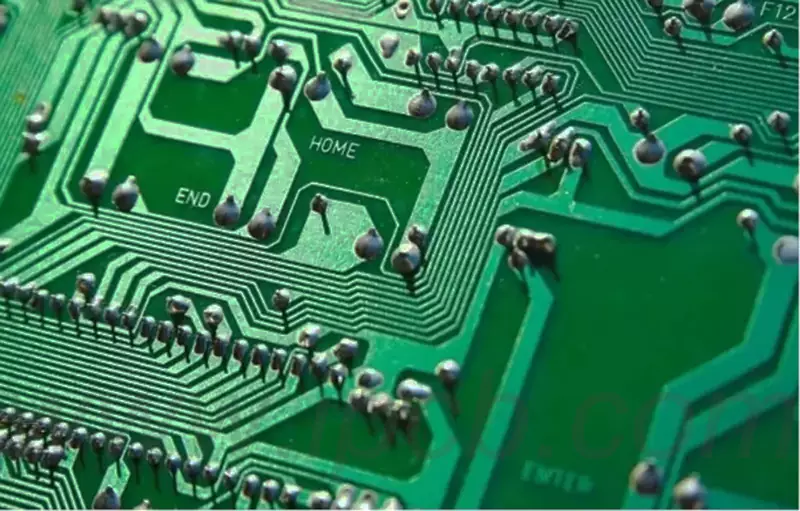
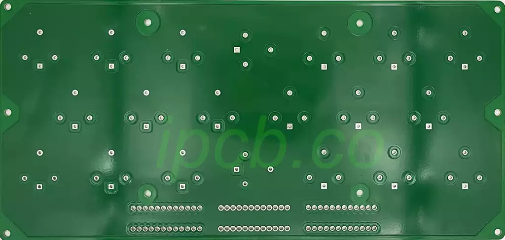
High Current PCB is circuit board designed specifically for the needs of high current applications. Compared to standard boards,they are characterised by thicker layers of copper, wider wires and excellent thermal conductivity, which allows for more efficient management and distribution of high-current loads. These boards are used in a wide range of applications such as power supply equipment, industrial automation controls, automotive electronics,and communication devices.
Design and construction of high current PCB
PCB Substrate Material Selection
Choosing the right PCB substrate material is critical; FR-4 is widely used as a conventional material, but when faced with high temperature environments, ceramic or metal substrates are preferred as they offer superior thermal performance and mechanical strength.
Copper Fill and Copper Layer Design
The use of Copper Pour and Copper Planes is critical in the design of high current PCB to increase current carrying capacity. These techniques reduce current density by increasing the area of copper on the PCB, which in turn reduces heat generation and voltage drop.
Alignment Specification Optimisation
High current PCB has a significantly higher alignment gauge than normal PCBs, which are typically wider and thicker. This is designed to conduct high currents more efficiently while avoiding increased resistance. Copper layers are typically between 2 ounces (oz) and 10 ounces thick, and may be even thicker.
Thermal Management Strategies
In high current PCB, thermal management issues cannot be ignored. In addition to the use of thick copper and wide alignments, strategies such as heat sinks, thermal pads, and thermal vias in PCB design are widely used to effectively dissipate heat and prevent overheating.
Application of Through-Hole Technology
Through-hole technology (THT) still occupies a key position in high current PCBs.It enables more reliable mechanical and electrical connections,especially in application scenarios that require high reliability and high current carrying capacity.
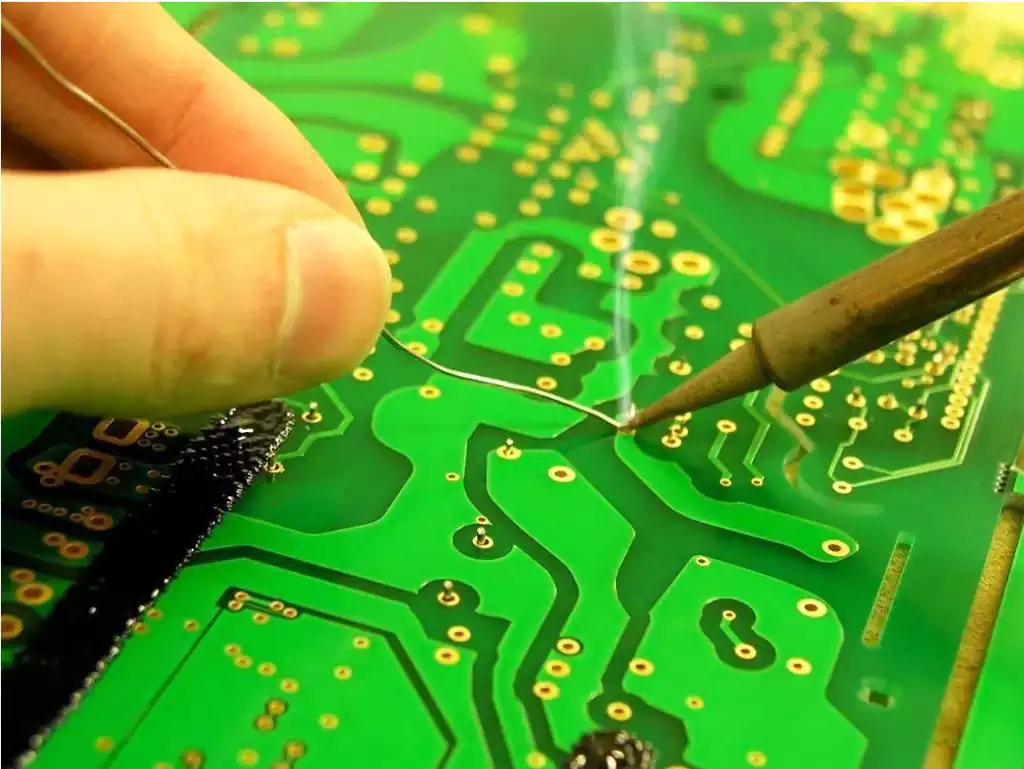
Soldering Process Requirements
During the soldering process of high current PCBs, special care must be taken to ensure that all connections can withstand high current shocks.Therefore,it is crucial to choose the right solder and soldering method (e.g. wave soldering or selective soldering),which can significantly improve the reliability of the connections.

High current pcb design elements to consider
- Current carrying capacity planning: The first task is to define the current carrying capacity of PCB alignments and components to prevent overheating and damage. This usually involves accurately calculating the width of the alignment to ensure that it can safely conduct the expected current.
- Alignment Size Setting: The size of the alignment needs to be determined based on the current value and allowable temperature rise. Generally speaking, the wider the alignment, the lower the resistance and the less heat generation.
- Alignment layout strategy: In high-current design, the length of the alignment should be shortened as much as possible and the bending should be reduced in order to lower the resistance and inductance, thus reducing the voltage drop and suppressing electromagnetic interference.
- Heat dissipation structure design: Given that high current generates a lot of heat, heat dissipation design is particularly critical. Heat dissipation can be enhanced through the use of large-area copper foil, heat sinks or heat sinks and other means.
- Vias and Pad Planning: Vias and pads need to be designed large enough to meet the challenge of high currents. In addition, the vias should be as close as possible to the component pads to reduce resistance and thermal resistance.
- Component Selection Considerations: Components that can withstand high currents, such as power MOSFETs, IGBTs, or high-current diodes, should be selected.
- Power and ground plane use: In multilayer board design, the introduction of power and ground plane can provide a low-impedance path to help reduce the voltage drop and improve power stability.
- Electromagnetic compatibility (EMC) management: high-current circuits are prone to electromagnetic interference, so measures need to be taken to reduce EMI, such as the use of shielding, filters and reasonable wiring techniques.
- Matching the coefficient of thermal expansion: In high-current applications, you also need to consider the coefficient of thermal expansion of the material, because the thermal expansion of different materials can lead to mechanical stress and connection problems.
- Safety Code Compliance: Relevant safety standards and codes, such as UL standards, must be adhered to, ensuring that the design meets industry safety requirements.
- Testing and validation: After the design is completed, comprehensive and in-depth testing and validation is required, covering thermal performance testing, electrical performance testing and reliability testing.
- Design Optimisation Iteration: According to the test results, necessary design iterations are carried out to optimise the alignment, component layout and heat dissipation design to meet the actual needs of high-current applications.
Fundamentals of High Current PCB Layout
There are some excellent examples of high current PCB designs that do not actually need to operate in a high voltage environment. Furthermore, the concepts of ‘high voltage’ and ‘high current’ are somewhat relative and subjective. A more appropriate indicator to distinguish between these design types might be safety. Where DC current poses a risk of electrocution or overheating, you may need to adopt some design principles to ensure the safety and reliability of your product.
Component Screening
In high-current designs and power systems, component reliability is often critical to overall reliability. Whilst this may seem obvious, it is vital to ensure that safety margins are taken into account when selecting components. In general, the following two specifications should be prioritised:
One is the current rating, especially for critical components such as MOSFETs and inductors;
The second is the thermal resistance value (if any).
You can either calculate the power consumption based on the estimated or designed operating current, or refer to the first specification above to get the worst-case current value. Both methods help to implement effective thermal management, which usually involves using the thermal resistance value to predict temperature. For some components, you can determine whether you need to add a heat sink to ensure their reliability.
In addition, in high current pcb, other important components such as connectors may have extremely high ratings and play a critical role in the power system.
Selecting the right copper thickness
The copper used in the alignment induces certain DC power losses, which are released as heat. This is particularly important for designs with very high currents, especially if the components are densely distributed. In order to reduce DC losses in high current PCB, an increase in the cross-sectional area of the copper conductor can be used. This means that either thicker copper needs to be used, or the alignment needs to be widened to keep Joule heat and power losses low enough. Using the PCB alignment width vs. current table, the copper thickness and/or alignment width required to avoid excessive temperatures can be determined.
Increasing Capacity: Using Flat Alternative Wires
If your power supply system needs to withstand extremely high current inputs and the width of a normal conductor is not sufficient for this, consider replacing the conductor with a power plane. For example, in our past Eurocard specification backplanes, we have used multiple power layers to carry 100A of current from two dedicated low voltage (24V) supplies. You can use this strategy in other systems as well when faced with the need to carry extreme currents.
Copper Cladding and Thermal Vias
With poor airflow inside the board enclosure, it can be difficult to remove heat from the device if you rely only on conduction or natural convection to dissipate the heat. In this case, thermal vias can be provided on circuit boards with copper cladding on the surface layer, through which a direct connection is established to a planar layer (e.g. GND), thus providing an additional transfer path for the heat away from certain heat-generating components. This method is particularly suitable for circuit areas close to hot components or high current alignments and can provide an additional conduction path for heat away from the surface layer. Note, however, that heat sinks should be avoided where electrical isolation is required, such as between the primary and secondary windings of a power transformer.
Whilst heat sinks can be useful for dissipating heat from specific components, a more comprehensive strategy is to think about using large heat sinks or direct conduction paths to the enclosure to achieve more efficient heat dissipation.
Emphasis on grounding design
High-current systems may require similar fail-safe precautions. A degree of safety and electromagnetic compatibility (EMC) can be achieved through proper grounding design. Generally, split earthing is not recommended, with the exception of power systems involving high currents and/or high voltages. In these systems, earthing needs to be handled separately between the input AC, unregulated DC and regulated DC sections.
A sensible starting point is the earthing scheme in AC systems or isolated power supplies. For high-current power systems, a three-wire DC configuration (PWR, COM, GND) is often used, where the GND connection is actually the ground connection. In such systems, the board may use an isolation strategy where the output side is disconnected from GND and the input side is grounded to ensure safety in the event of a fault.
Choose a thicker board
This may seem counterintuitive at first. One might think that a thinner board would provide better thermal conduction away from heat-generating components, so why choose a thicker board? In fact, when a circuit board of a non-standard thickness is used, its in-plane thermal resistance decreases while the board’s heat capacity increases. In addition, thicker boards (e.g. 2 mm or 3 mm) provide better mechanical support for large components in high-current boards, especially inductive components and large heat sinks mounted on the board.
Electrostatic Discharge (ESD) and Safety Considerations
DC sections present a unique set of issues, particularly in power systems, especially those designs that need to withstand both high voltages and high currents.
Advantages of High Current Thick Copper PCBs.
Enhanced durability and structural robustness
Thick copper PCBs are structurally more robust and can withstand higher mechanical stresses, thus extending the overall life of the PCB.
Enhanced Current Conduction
By increasing the thickness and area of copper, thick copper PCBs significantly increase current carrying capacity, making them ideal for high current applications.
Optimised Electrical Performance
Thick copper PCBs have lower resistance and inductance, which contributes to the efficiency and overall performance of the circuit.
Improved Thermal Control
Thick copper PCBs have excellent thermal conduction characteristics, which allows for more effective heat dissipation and prevents overheating, enhancing PCB reliability.
Increased Design Flexibility
Thick copper PCBs provide designers with greater flexibility to meet the needs of a wide range of applications, such as power modules and automotive electronics.
Optimised power distribution
Thick copper PCBs distribute power more evenly, reducing voltage drop and current density, thus improving the overall efficiency of the circuit.
Cost-effective and space-efficient
Through clever design and material selection, thick copper PCBs can achieve cost savings and space optimisation in certain applications, providing a more compact design solution.
Wide range of applications
Thick copper PCBs are widely used in many fields such as power supply equipment, industrial control, automotive electronics, communication equipment, etc., and are able to meet a variety of high current requirements.
The design of high current pcb requires comprehensive consideration of many factors,and thick copper PCBs are the preferred choice for high-current applications due to their advantages. Attention to detail and optimisation to ensure product performance and quality to meet the growing demand for applications.


