Below is a precise, idiomatic, and industry-appropriate English translation suitable for use in PCB engineering documentation, technical white papers, or professional marketing materials.Thanks to its mature manufacturing ecosystem and excellent cost performance, FR4 has long dominated the PCB substrate market. However, as signal frequencies climb into the GHz range, signal-integrity challenges in FR4 routing are becoming increasingly pronounced. Reflection, crosstalk, and attenuation occur more frequently, and the root cause of these issues often converges on one fundamental problem: loss of impedance control.
Controlled impedance is not an exclusive technology reserved for high-end RF laminates. With disciplined design methodologies and robust process control, standard FR4 can also achieve accurate impedance matching, enabling stable and reliable high-frequency signal transmission.
Relationship Between Controlled Impedance and Signal Integrity in FR4 Routing
Signal transmission on a PCB is essentially the propagation of voltage and current waveforms. Impedance represents the ratio between voltage and current and directly governs transmission behavior. For general-purpose substrates such as FR4, impedance stability is tightly coupled to signal integrity. When trace impedance is properly matched to the source and load, signal energy is transmitted efficiently with minimal reflection or loss. Conversely, impedance discontinuities cause reflections at transition points, forming standing waves that distort signals, exacerbate crosstalk, and reduce data rate and transmission distance.
The intrinsic material characteristics of FR4 make impedance control more challenging. Compared with high-frequency laminates such as Rogers materials, FR4 exhibits inherent dielectric constant (Dk) variability. Standard FR4 typically has a Dk of 4.2–4.8, and even low-loss FR4 shows Dk variation of ±0.2 across frequency ranges of 1–10 GHz and temperature ranges of –40°C to 85°C. In addition, FR4 has higher dielectric loss (Df), which accelerates signal attenuation at high frequencies. These factors make FR4 routing more prone to impedance deviation. Consequently, the essence of impedance-control optimization lies in offsetting FR4’s inherent material limitations through targeted design and process strategies, achieving accurate impedance matching and stable signal transmission.
Different application scenarios impose different impedance-tolerance requirements. For consumer electronics Wi-Fi 6 routing, impedance tolerance can be ±10%. For industrial IoT high-frequency data links, tolerance must be tightened to ±8%. For core RF routing in 5G Sub-6 GHz terminals, tolerance requirements are typically ≤±5%. The objective of controlled impedance design is to keep trace impedance within the required tolerance window despite the inherent constraints of FR4.
Primary Causes of Impedance Loss of Control in FR4 Routing
1.Substrate Property Variability
Dielectric constant variability is the most fundamental cause of impedance instability in FR4. Dk is strongly influenced by resin content, glass fabric style, and lamination conditions. A 5% variation in resin content can cause a ±0.3 shift in Dk. In FR4 laminates combining 7628 and 2116 glass fabrics, regional Dk differences can reach 0.4. Insufficient lamination temperature or pressure can lead to uneven resin distribution, creating localized Dk variations. Because trace impedance is inversely proportional to the square root of Dk, even small Dk fluctuations can cause significant impedance deviation.
Dielectric thickness uniformity is another critical factor. Uneven pressure during lamination can introduce thickness variations of up to ±10%. Since impedance is proportional to the square root of dielectric thickness, thickness deviation directly translates into impedance error. For example, if a design targets a dielectric thickness of 1.6 mm but the actual thickness drops to 1.44 mm, impedance increases by approximately 7%, exceeding the ±5% tolerance required for precision applications.
2.Routing Design Deficiencies
Design-level oversights are a major human-driven cause of impedance discontinuities. Many engineers focus only on basic trace width and spacing while overlooking finer design details that significantly affect impedance.
Abrupt trace-width changes are the most common issue. In high-frequency routing, sudden widening or narrowing of traces causes corresponding impedance changes—wider traces reduce impedance, narrower traces increase it—resulting in reflections. On FR4, where Dk variability is already significant, reflected signals can superimpose and severely degrade signal quality. Right-angle bends, poorly designed vias, and branch stubs also introduce localized impedance discontinuities. A conventional 90-degree corner effectively increases trace width, locally reducing impedance by 5–8%. Unmatched vias introduce parasitic capacitance and inductance, forming major reflection points along the signal path.
3.Manufacturing Process Deviations
Even with precise impedance calculations at the design stage, manufacturing variations can still shift impedance. Key PCB fabrication processes—including etching, solder mask application, and lamination—directly affect routing impedance.
Etching variation is the most influential factor. Over-etching narrows traces and increases impedance, while under-etching widens traces and lowers impedance. Standard etching processes may introduce trace-width deviations of up to ±0.05 mm. For a 50-ohm microstrip on FR4 with a dielectric thickness of 1.6 mm, a 0.05 mm width deviation can cause an impedance shift of approximately ±6%, exceeding tight tolerance requirements. Solder mask application also affects impedance. Solder mask ink has a dielectric constant of approximately 3.0–3.5, and non-uniform thickness alters the effective dielectric environment. In some cases, solder mask coverage increases transmission loss on high-frequency traces.
4.Environmental Influences
The operating environment further affects impedance stability. Temperature and humidity changes alter FR4 material properties and indirectly cause impedance drift.
As temperature increases, FR4’s Dk decreases while dielectric thickness increases due to thermal expansion, with both effects driving impedance upward. Experimental data show that standard FR4 exhibits impedance variation of approximately ±7% across –40°C to 85°C. In high-temperature industrial environments (85°C–125°C), variation can expand to ±10%. Humidity effects stem from FR4’s hygroscopic nature. Absorbed moisture, with a dielectric constant of approximately 80, increases the effective Dk and lowers impedance. After 24 hours at 85% relative humidity, FR4 trace impedance can decrease by 3–5%.
Core Pathways to Improving FR4 Routing Performance Through Controlled Impedance
1.Optimized Material Selection
Selecting the appropriate FR4 grade is the foundation of impedance control. Material choice should be aligned with signal frequency, temperature range, and impedance-tolerance requirements.
For high-frequency applications (2.4–10 GHz), low-loss FR4 with reduced Dk variability is preferred. These materials use modified epoxy resins and high-performance glass fabrics, achieving Dk values of 3.8–4.2 and Df as low as 0.008–0.012, with Dk variation reduced to ±0.1. For high-temperature environments such as industrial control or automotive electronics, high-Tg FR4 (Tg ≥170°C) is recommended due to superior thermal stability and reduced impedance drift.
Dielectric thickness uniformity must also be controlled. Suppliers with mature lamination processes should be selected, with thickness tolerance ≤±5%. For precision high-frequency projects, suppliers should provide measured Dk data for impedance calculation. Incoming FR4 materials should be pre-baked (120°C for 2–4 hours) to reduce moisture content and minimize humidity-induced impedance variation.
2.Precision Routing Design
Routing design is the core of impedance control and must address trace geometry, topology, and via implementation.
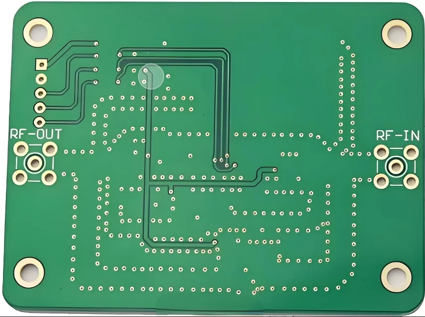
Accurate trace-width and spacing calculation is fundamental. Based on target impedance (e.g., 50 Ω or 75 Ω), FR4 Dk, and dielectric thickness, precise dimensions should be calculated using impedance tools such as Polar SI9000. For example, with a target impedance of 50 Ω, Dk = 4.2, and dielectric thickness of 1.6 mm, a microstrip trace width is approximately 3.2 mm, while a stripline width is about 2.8 mm. Manufacturing compensation of 0.02–0.03 mm should be added to account for etching variation.
Topology optimization is essential to maintain impedance continuity. High-frequency routing should follow a “straight-line first, gradual transition” principle. Right-angle corners should be avoided in favor of 45-degree chamfers or curved bends. Where width transitions are unavoidable, a tapered section at least three times the trace width should be used. Branch stubs should be minimized, favoring daisy-chain or point-to-point topologies. Via impedance must be addressed through blind/buried vias, ground-copper shielding around vias, and simulation-driven optimization of via diameter and pad size.
3.Manufacturing Process Control
Process control translates design intent into real-world impedance accuracy. Etching, solder mask, and lamination must be tightly controlled.
Etching control focuses on trace-width precision. A dry-film plus acidic etching process, combined with optimized chemistry, temperature, and dwell time, can limit width deviation to ±0.02 mm. Statistical process control (SPC) should be implemented for real-time monitoring. For solder mask, selective solder mask is preferred to avoid covering high-frequency traces. If coverage is required, thickness variation should be limited to ±0.01 mm.
Lamination control focuses on dielectric thickness uniformity. Optimized temperature, pressure, and cycle time should ensure thickness tolerance ≤±5%. Post-lamination thickness inspection is essential, with out-of-spec panels rejected. Drilling accuracy also affects via impedance and should be controlled to within ±0.01 mm.
4.Simulation-Driven Verification and Iteration
Controlled impedance design for high-frequency FR4 relies heavily on simulation. Tools such as HFSS or CST enable early identification of impedance discontinuities and reduce costly rework.
During material selection, simulation can compare impedance stability across different FR4 grades. During design, key signal paths should be simulated to identify impedance discontinuities and optimize geometry and vias. During process validation, actual manufacturing parameters—such as post-etch trace width and laminated dielectric thickness—should be fed back into simulation to refine compensation values.
Before mass production, prototype boards should be fabricated and measured using impedance testers. Simulation and measurement results should be compared, and deviations analyzed. For example, if measured impedance is 5% higher than simulated, trace width can be increased by approximately 0.03 mm or dielectric thickness adjusted to achieve target impedance.
5.Enhanced Environmental Robustness
Design and process strategies should address environmental impacts on impedance stability.
For high-temperature applications, high-Tg FR4 should be complemented with additional copper planes for heat dissipation, and impedance margin should be reserved through simulation. For high-humidity environments, low-moisture-absorption FR4 (≤0.2%) should be selected, and conformal coating applied to reduce moisture ingress. For vibration- and shock-prone applications such as automotive or industrial equipment, mechanical PCB design should prevent deformation-induced impedance variation, and reinforced via structures should be used to maintain via stability.
Optimized Impedance-Control Solutions for Different High-Frequency FR4 Applications
1.Consumer Electronics Wi-Fi 6/6E (2.4–7.125 GHz)
Characteristics: Moderate frequency, ±10% impedance tolerance, cost-sensitive, operating temperature –10°C to 60°C.
Solution: Low-loss FR4 (Dk 3.8–4.2, Df ≤0.01); microstrip routing with precise width calculation and 0.02 mm etch compensation; 45-degree bends; standard through-vias with minimized pad parasitics; etch width control ≤±0.03 mm; no selective solder mask to balance cost and performance.
2.Industrial IoT High-Frequency Data Links (5–10 GHz)
Characteristics: Higher frequency, ±8% tolerance, high reliability, –40°C to 85°C, vibration exposure.
Solution: High-Tg low-loss FR4 (Tg ≥170°C, Dk 3.8–4.0); stripline routing for improved stability and EMI immunity; simulation-driven geometry with 0.02 mm compensation; blind/buried vias; selective solder mask; added thermal copper and reinforced vias; impedance verification across temperature extremes prior to mass production.
3.5G Sub-6 GHz Core RF Paths (3.5–6 GHz)
Characteristics: Tight ±5% tolerance, extreme signal-integrity requirements, –20°C to 70°C.
Solution: High-precision low-loss FR4 with Dk variation ±0.1 and Df ≤0.008; supplier-provided measured Dk data; microstrip routing with ±0.01 mm width tolerance; simulation-optimized spacing and ground clearance; impedance-matched vias with shielding; high-precision etching (≤±0.01 mm); selective solder mask; full-path simulation and measurement; conformal coating for environmental robustness.
In a cost-sensitive electronics market, FR4’s cost-performance advantage remains irreplaceable. Mastering the core principles of controlled impedance optimization not only enhances FR4’s high-frequency performance but also maximizes cost efficiency, achieving an optimal balance between performance and budget. As FR4 material technology continues to evolve toward lower Dk variability and higher stability, and as design and process precision further improve, the application boundaries of FR4 in high-frequency domains will continue to expand—delivering more cost-effective solutions to the electronics industry.