With the rapid proliferation of electronic products and the swift advancement of technology, demand for high-frequency, high-speed printed circuit boards continues to grow. High frequency PCB plays a pivotal role in modern communications, radar systems, and high-speed data processing. However, their unique high-frequency characteristics and stringent requirements for signal integrity render the manufacturing of high-frequency PCBs a challenging undertaking. This paper will delve into the key challenges in high frequency PCB design and manufacturing, proposing corresponding solutions.
For high-frequency applications, techniques for high frequency PCB design within board interconnections include:
- Employing 45-degree angles at transmission line corners to minimise return loss.
- Utilising high-performance dielectric boards with strictly controlled dielectric constants by layer. This facilitates effective management of electromagnetic fields between dielectric materials and adjacent routing.
- Refine PCB design specifications concerning high-precision etching. Consider stipulating a total line width tolerance of ±0.0007 inches. Manage undercuts and cross-sections of trace geometries while specifying plating conditions for trace sidewalls. Comprehensive management of trace geometry and coating surfaces is crucial for addressing skin effect issues at microwave frequencies and achieving these specifications.
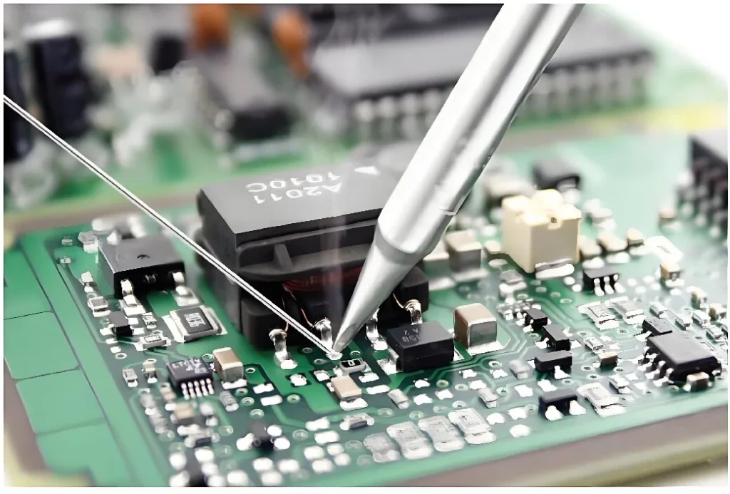
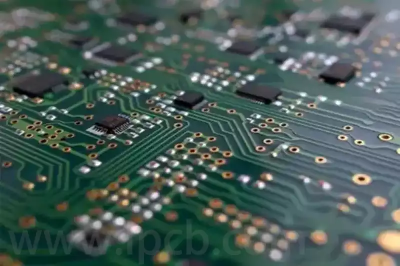
- Lead wires introduce tap inductance; components with leads should be avoided. Surface-mount components are preferable in high-frequency environments.
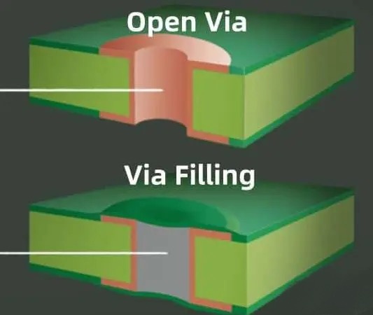
- For signal vias, avoid using plated-through hole (pth) processes on sensitive boards. This process introduces lead inductance at the via location. For instance, a single via on a 20-layer board connecting layers 1 to 3 may affect lead inductance across layers 4 to 19.
- Provide ample ground planes. Connect these ground planes using moulded vias to mitigate the effects of three-dimensional electromagnetic fields on the circuit board.
- Select non-electrolytic nickel plating or immersion gold plating processes; avoid HASL plating. This plating surface provides superior skin effect properties for high-frequency currents. Furthermore, this highly solderable coating requires fewer leads, contributing to reduced environmental pollution.
- Solder resist prevents solder paste migration. However, due to thickness uncertainty and unknown insulation properties, covering the entire board surface with solder resist causes significant electromagnetic energy variations in microstrip designs.Solder dams are typically employed as the solder resist layer.
With the rapid proliferation of electronic products, demand for high frequency pcb, high-speed printed circuit boards continues to grow. Nevertheless, manufacturing such boards presents considerable challenges with numerous technical hurdles.
Solutions:
- Material Selection
The choice of materials for high-frequency, high-speed printed circuit boards is critical. Material properties directly influence the pcb board’s high-frequency transmission performance and signal-to-noise ratio. Typically, materials must exhibit low loss factor, high dielectric constant, and excellent thermal stability. Therefore, material selection requires careful consideration. - Manufacturing Process
The manufacturing process for high-frequency, high-speed printed circuit boards is paramount, as its quality directly determines the board’s performance. During production, precision control and technical expertise are essential to ensure the accuracy and quality of the printed circuit board. At the design stage, meticulous attention must be paid to the precise positioning of every conductor, via, and pad. - Layer Stackup
The layer stack-up of high-frequency, high-speed printed circuit boards presents significant challenges. Typically, factors such as board thickness, dielectric material type, copper foil thickness, and stacking configuration must be considered during layer stack-up design. - Stress Relief Treatment
During the manufacturing process of high-frequency, high-speed printed circuit boards, stress relief treatment is required to eliminate internal stresses. However, improper execution of this step can severely compromise the board’s performance. Typically, thorough analysis and calculation of materials, board thickness, layer stacking configuration, trace width, and pad diameter must precede abnormal thermal treatment. - Trace Routing
Trace routing constitutes a critical phase in high-frequency, high-speed PCB fabrication. Improper routing adversely affects the board’s high-frequency performance and signal-to-noise ratio. During routing, adherence to the principle of separating signal and power traces is essential. Strict control over coating thickness, layer spacing, and interconnections between planes and layers is required.
The design and manufacture of high frequency PCB constitutes a complex and precision-demanding engineering endeavour. Overcoming these challenges necessitates meticulous management and innovation from engineers. Through a series of optimisation measures, the performance and reliability of high-frequency PCBs can be significantly enhanced, thereby driving the advancement of electronic products towards higher performance and smaller form factors.