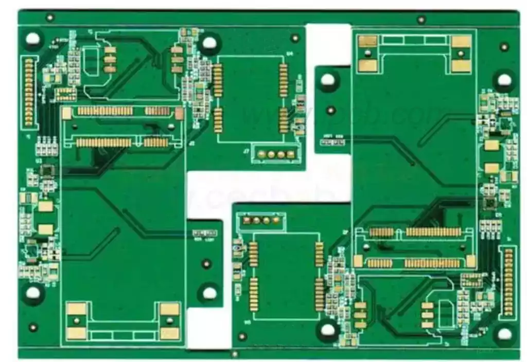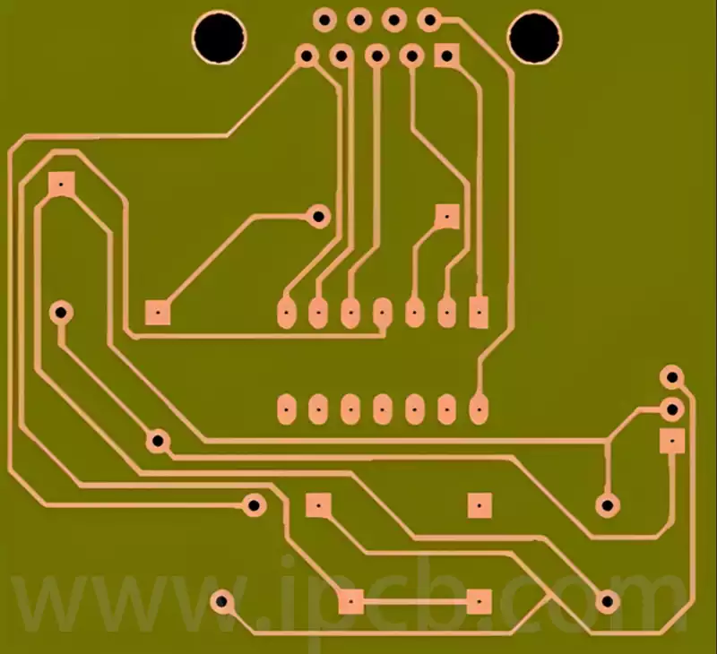
A pcb prototype board should do more than prove that a circuit can power on. It should reveal whether the design can be fabricated, assembled, programmed, tested and reproduced without creating avoidable problems during production.
If a pcb prototype board is evaluated only for basic functionality, manufacturing weaknesses may remain hidden until a larger order is released. The result can be poor assembly yield, unstable component sourcing, difficult testing or repeated design revisions after production tooling has already been purchased.
A Working Circuit Is Not Yet a Production Ready Design
An engineering prototype may operate correctly even when it contains hand-soldered components, temporary wires or manually corrected connections. These modifications are acceptable during early debugging, but they do not demonstrate that the same result can be produced consistently on an automated manufacturing line.
A useful pcb prototype board must distinguish between a design that works once and a design that can be repeated. This means recording every modification, verifying the final component values and confirming that the manufacturing files represent the board that was actually tested.

When engineers correct a prototype without updating the schematic, BOM and PCB layout, the next production batch may reproduce the original defect. Every successful change made to the pcb prototype board should therefore return to the controlled design data.
Manufacturing Data Must Describe One Consistent Revision
PCB manufacturers normally require Gerber or ODB++ data, drill files, a board drawing and fabrication notes. Assembly requires additional information such as the BOM, component coordinates, polarity markings and assembly drawings.
These files must describe the same revision. A modified Gerber file combined with an older drill file can produce missing or misplaced holes. A current PCB layout paired with an outdated BOM can cause incorrect components to be purchased and installed.
Before ordering a pcb prototype board, the manufacturer should check the data package for conflicting dimensions, missing layers, unclear stack-up information and unsupported tolerances. The review should also confirm whether special requirements such as controlled impedance, filled vias, specific copper weights or surface finishes are clearly identified.
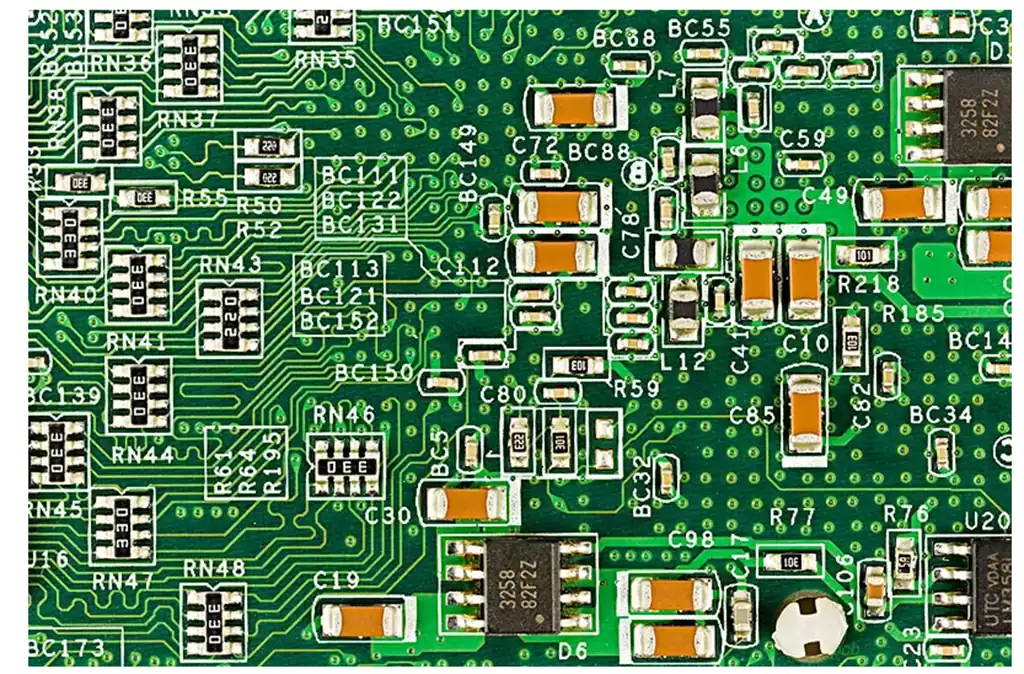
IPC’s PCB assembly checklist connects data transfer, board design, land patterns, thermal management, stencil design and component placement with their relevant standards. This illustrates why prototype evaluation should consider the complete manufacturing process rather than the PCB image alone.
Fabrication Choices Must Be Tested Under Real Conditions
Material, copper thickness, layer structure, surface finish and via technology affect both performance and manufacturing cost. Selecting these features from a capability table does not confirm that they are appropriate for the product.
For example, a high-speed circuit may require controlled impedance, while a power circuit may depend on copper thickness and thermal spreading. Fine-pitch BGAs may require microvias or via-in-pad structures, but adding HDI features without a routing need can make the board unnecessarily expensive.
The pcb prototype board should use the intended production stack-up whenever electrical performance depends on layer spacing or reference-plane position. Replacing the production structure with a convenient prototype stack-up can produce misleading results in signal integrity, impedance and electromagnetic behaviour.
Manufacturing tolerances should also be realistic. IPC design standards describe different producibility levels representing increasing process difficulty and cost. Critical features should be selected according to the product’s actual requirements instead of automatically applying the smallest available trace, spacing or hole size throughout the design.
Prototype Assembly Exposes Process Weaknesses
The assembly stage often reveals problems that are not visible in the bare PCB data. Component footprints may have incorrect pad dimensions, polarity markings may be unclear, connectors may interfere with the enclosure and closely spaced components may prevent effective inspection or rework.
Solder-paste behaviour is especially important for fine-pitch components and bottom-terminated packages. Pad geometry, stencil apertures, paste volume, placement accuracy and reflow temperature interact with one another. A pcb prototype board that requires repeated manual correction may indicate that the assembly process window is too narrow.
Prototype PCB assembly should use the intended component packages and a representative soldering process. If the prototype is assembled entirely by hand while production will use stencil printing and automated placement, certain manufacturability problems may not appear.
Inspection results should be documented rather than described only as a pass or failure. Insufficient solder, bridging, voiding, component movement and tombstoning each point to different underlying causes. Evaluating these patterns allows the pcb prototype board to improve the design before the same defect is repeated across a larger batch.
IPC-A-610 provides visual acceptability requirements for electronic assemblies, while J-STD-001 defines requirements for soldered electrical and electronic assemblies. The applicable acceptance class and any customer-specific requirements should be agreed before prototype inspection begins.
Component Availability Is Part of Prototype Validation
A circuit cannot enter stable production if its essential components cannot be purchased reliably. Prototype builds sometimes use available substitutes because the preferred part has a long lead time. This can accelerate engineering work, but the substitution must be controlled.
Every component fitted to a pcb prototype board should be compared with the approved BOM. If an alternative part is used, its package, electrical ratings, temperature range, lifecycle status and firmware compatibility should be reviewed.
This is particularly important for microcontrollers, power devices, memory, wireless modules and connectors. Two parts with similar headline specifications may behave differently during startup, thermal loading or communication. Alternative components should be validated during the prototype stage instead of being introduced after production begins.
Testing Must Represent Product Operation
Powering the board and observing one output does not provide sufficient test coverage. A production-oriented test plan should verify important power rails, current consumption, communication interfaces, analogue signals, sensors, outputs and protection functions.
Test access must also be examined on the pcb prototype board. Programming pads, ground points and critical signals need to remain accessible after assembly. If test points are removed to save space, production troubleshooting may become slow or dependent on manual probing.
Functional PCB testing should reproduce relevant operating conditions. A motor controller may need testing under load, a wireless board may require communication and RF checks, and a sensor interface may need calibrated input signals. Thermal behaviour should be observed after the board has operated long enough to reach a stable temperature.
Results from the pcb prototype board should become the basis for production test limits. Recording measured values instead of relying only on a visual pass indicator makes it easier to identify units that technically operate but fall outside the expected performance range.
Revision Control Turns Prototype Findings Into Improvements
Prototype feedback has little value if it remains in emails, handwritten notes or reworked samples. Each issue should be connected to its cause, corrective action and design revision.
A pcb prototype board review should compare the schematic, PCB files, BOM, assembly data, firmware and test procedure. When one item changes, its effect on the other documents must be checked. This prevents a corrected PCB from being combined with obsolete purchasing or programming information.
At iPCB, prototype fabrication and assembly can be combined with DFM, BOM and testability reviews before low volume PCB production begins. Using one controlled revision across fabrication, sourcing and assembly helps ensure that the tested prototype corresponds to the data released for the next build.
Moving From Prototype to Production
A successful prototype build should close the gap between engineering intent and manufacturing reality. Before production release, the team should confirm that design modifications are documented, components are approved, assembly defects are understood and the test method can be repeated without relying on the original engineer.
The pcb prototype board should also be produced with materials and processes that reasonably represent the planned product. A prototype that depends on exceptional manual skill or temporary parts may demonstrate the circuit concept, but it does not yet demonstrate production readiness.
The real value of a pcb prototype board is not that it produces one working sample. Its value lies in discovering fabrication, assembly, sourcing and testing risks while they are still inexpensive to correct. When those findings are incorporated into controlled production files, the prototype becomes evidence that the design can be manufactured consistently rather than merely proof that the circuit can operate.