As the power density of electronic systems continues to increase, thermal management has become one of the core factors constraining product performance and reliability. Within traditional FR-4 PCB architectures, the substrate’s inherently limited thermal conductivity makes it difficult to dissipate heat generated by components promptly and efficiently. Consequently, systems often rely on external heat sinks, thermal pads, or even active cooling methods to control temperature rise. However, numerous practical engineering applications demonstrate that ceramic PCBs frequently achieve long-term stable operation without additional heat sinks. This stems not from lower component power consumption, but from fundamental differences in material composition and structural design.
Material-wise, ceramic PCBs typically employ alumina, aluminium nitride, or silicon nitride as substrates. These materials exhibit typical inorganic crystalline structures, with lattice vibration-based heat transfer efficiency far surpassing that of organic resin systems. Notably, aluminium nitride and silicon nitride not only possess excellent electrical insulation properties but also demonstrate significantly superior thermal conductivity compared to FR-4. This enables them to directly undertake the primary task of conducting heat away from the chip area to the external environment.
Consequently, within ceramic PCB architectures, the substrate transcends its role as a mere passive carrier layer for electrical interconnections, evolving into a critical component of the thermal management system. Heat dissipation functionality is integrated directly into the PCB body, reducing reliance on external heat sinks from the design inception.
Further analysis of thermal conduction pathways reveals inherent structural flaws in the heat dissipation mechanisms of traditional organic PCBs like FR-4. Heat generated by power devices must sequentially traverse the chip body, solder layer, copper foil, resin-based dielectric layer, and rear structure before dispersing outward. This multi-layered, complex interface pathway presents significant thermal resistance bottlenecks, particularly due to the exceptionally low thermal conductivity of the resin dielectric layer. As the number of interfaces increases, interfacial thermal resistance and material thermal resistance accumulate, progressively “diminishing” heat during conduction. This ultimately causes heat to accumulate in localised areas of the device, leading to rapid junction temperature rise. Consequently, traditional PCB architectures often compensate for their inherent thermal limitations only through the addition of heat sinks or active cooling methods.
At the structural level, ceramic PCBs fundamentally transform this heat transfer paradigm. The core lies in the DBC (Direct Bonded Copper) or AMB (Active Metal Brazing) process, which establishes a metallurgical-grade direct bond between the thick copper layer and the ceramic substrate, rather than relying on mechanical adhesion via resin or adhesive layers. This metal-ceramic interface lacks any soft intermediate layer, resulting in extremely low interfacial thermal resistance. Consequently, heat can be transferred efficiently and stably from the copper layer into the ceramic substrate.
During operation, heat generated by power devices first traverses the solder or sintered layer into the upper thick copper conductor. It then conducts almost unimpeded vertically to the highly thermally conductive ceramic substrate, subsequently diffusing to the substrate’s rear surface. Compared to traditional PCBs requiring heat to ‘detour’ through low-thermal-conductivity dielectric layers, ceramic PCBs offer a far more direct thermal flow path, significantly reducing equivalent thermal resistance.
More crucially, this vertical thermal path is highly concentrated and predictable. Heat transfer from the device junction to the substrate’s rear surface follows an almost linear distribution, enabling system designers to precisely control junction temperature and thermal gradient distribution. Even without additional heat sinks, the ceramic substrate’s rear surface can reliably dissipate heat into the environment through contact with metal enclosures or natural convection.
In high-power applications, the true threat to reliability often stems not from overall temperature levels, but from the formation of localised hotspots. Abnormal temperature spikes near power chips, current-dense zones, or solder pads create pronounced thermal gradients, leading to concentrated thermal stress, accelerated solder joint fatigue, and electrical performance drift in components. These issues represent the critical pain points that traditional PCB architectures struggle to address effectively.
Ceramic PCBs employ a synergistic design combining thick copper layers with highly thermally conductive ceramic substrates, effectively suppressing localised hotspots through enhanced thermal diffusion mechanisms. Beneath power components, the thick copper layer first facilitates lateral heat dispersion. Compared to conventional thin copper foil, thick copper exhibits lower planar thermal resistance and higher thermal mass. This enables rapid planar heat spreading during the initial heat generation phase, preventing thermal concentration beneath individual pads or chips.
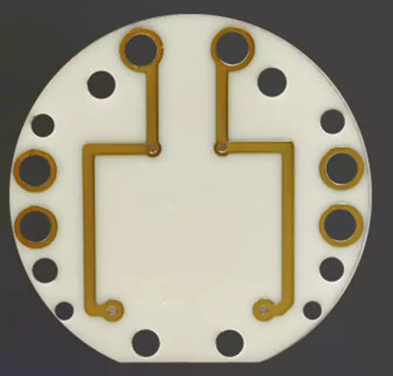
Concurrently, the high-thermal-conductivity ceramic substrate provides a stable, efficient thermal conduction pathway in the vertical direction. Once heat undergoes initial temperature equalisation through the thick copper layer, it rapidly conducts downward via the low thermal resistance copper-ceramic interface and is continuously dissipated by the ceramic substrate. This vertical thermal capability ensures heat does not stagnate within the copper layer, establishing a continuous, controllable heat dissipation pathway.
The lateral heat spreading capability of the thick copper layers synergises with the vertical thermal conductivity of the ceramic substrate to establish a three-dimensional thermal diffusion network. Heat neither accumulates in localised areas nor recirculates back beneath the device due to inadequate dissipation. This fundamentally reduces both peak temperatures and thermal gradients within the operational zone.
With localised hotspots effectively mitigated, the temperature distribution beneath the device becomes more uniform, significantly alleviating thermal stress concentration. This not only helps stabilise the device’s electrical performance parameters, preventing performance drift caused by temperature non-uniformity, but also markedly delays the thermal fatigue process of solder joints, metallisation layers, and packaging materials, thereby enhancing the overall system’s long-term reliability.
Ceramic PCBs resolve thermal challenges not through ‘external cooling’ but by reconfiguring thermal conduction and diffusion pathways through material and structural redesign. The combination of highly thermally conductive ceramic substrates, low thermal resistance metallisation structures, and the synergistic thermal equalisation mechanism between thick copper and ceramic enables rapid, uniform, and predictable heat dissipation.
It is precisely this systemic thermal management capability, originating from the PCB itself, that allows ceramic PCBs to reduce or even eliminate the need for traditional heat sinks in numerous high-power applications. This provides a more compact and stable solution for high-power-density, high-reliability electronic systems.
