From Organic Resin to Glass: Why Intel Sparked a “Materials Revolution” in Chip Substrates
In the history of semiconductor chip development, the renowned “Moore’s Law” has consistently guided the industry’s integration efforts at breakneck speed. However, as transistor sizes approached physical limits (e.g., reaching 2 nanometers or even smaller process technologies), squeezing space onto a single silicon wafer became increasingly difficult and costly.
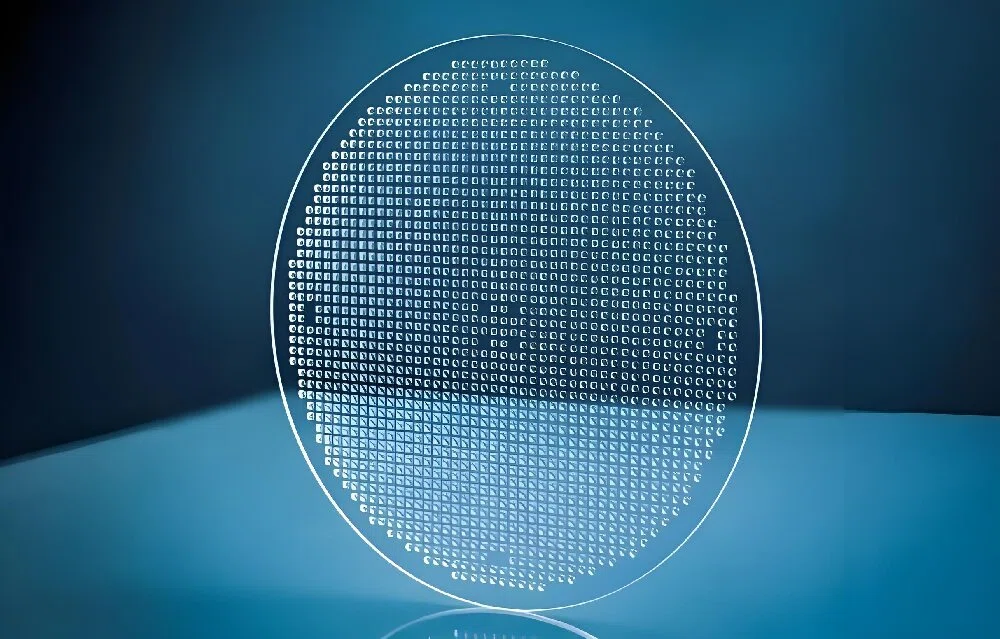
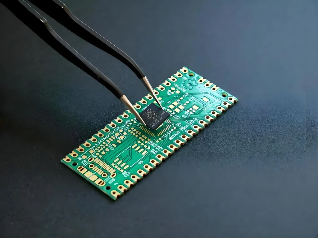
To break this deadlock, the entire semiconductor industry began a comprehensive shift towards “Advanced Packaging”—combining multiple small chips (chiplets) with different functions tightly onto a single substrate, like building blocks, to create a super chip. Against this backdrop, Intel’s high-profile debut of its Intel glass substrate undoubtedly dropped a bombshell on the entire electronics and integrated circuit manufacturing industry.
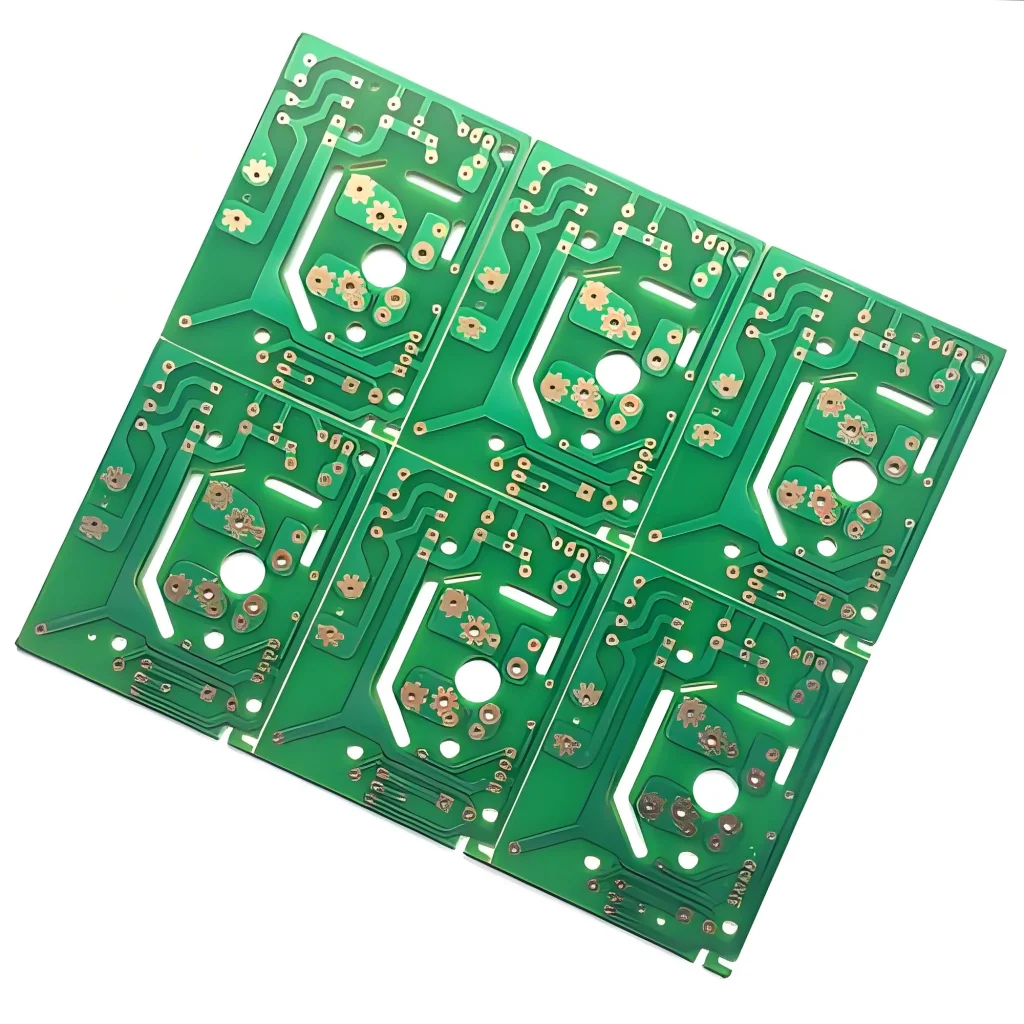
For a long time, whether manufacturing traditional PCB circuit boards or internal chip packaging substrates (ABF substrates), the core material has been organic resin (a mixture of plastic and epoxy resin). Intel’s proposed glass substrate technology directly signals the impending end of the dominance of organic materials, with glass becoming the ultimate foundation for future high-performance computing chips.
The Microscopic Physical Limits of Organic Substrates
Why have organic resin materials, used for decades, suddenly fallen out of favor in the high-end chip field?
Let’s clarify the logic through three fatal “physical ceilings”: First, the “soft collapse” caused by thermal expansion mismatch. As mentioned earlier, silicon in chips hardly expands when heated, but organic resin materials are essentially plastics, expanding significantly when heated. In the past, when chip power consumption was low and size was small, this difference was tolerable. However, current AI chips or data center processors consume hundreds or even thousands of watts, generating astonishing amounts of heat. Under this prolonged ultra-high temperature “baking,” organic substrates are prone to microscopic warping and bending. Once the substrate bends, the hundreds of thousands of tiny solder joints connecting the chip can be pulled apart or short-circuited.
Second, the material itself is not “hard” enough. To accommodate more tiny chips, future packaging substrates are becoming increasingly larger, even approaching massive sizes like 100*100 mm. Organic resins are very thin and flexible; however, when the area becomes large, they simply cannot provide sufficient rigidity to support the delicate silicon chips. During assembly and thermoforming, even slight stress will cause them to bend like potato chips.
Finally, and most critically, it cannot be used to create finer “micro-highways.” The surface of organic resins is uneven, full of microfiber burrs. When engineers attempt to use lasers to burn extremely tiny conductive holes or photolithography to create extremely fine copper wires, the surface roughness and water absorption deformation characteristics of the material directly lead to blurred and broken circuit edges. This results in the wiring density of organic substrates being capped at a certain limit, which can no longer be reduced.
The “Perfect Physical Properties” of Glass Materials
Because organic materials are riddled with dead ends in terms of performance, rigidity, and precision, Intel turned its attention to special glass with a mirror-like surface and unparalleled hardness. Compared to organic resins, glass substrates possess near-perfect physical and chemical advantages: their coefficient of thermal expansion is almost perfectly synchronized with that of silicon chips. Glass expands at an extremely low rate; even when the chip is heated to hundreds of degrees Celsius, the glass substrate maintains a remarkably synchronized expansion pace with the silicon chip. This completely solves the problem of solder joint breakage caused by thermal stress, dramatically increasing chip lifespan and reliability.
Simultaneously, glass possesses incredibly high flatness and rigidity. Even with the substrate area increased several times over and the thickness compressed to an extremely thin level, the glass remains as flat as a mirror, never bending or deforming. This allows fully automated placement machines to achieve unprecedented alignment precision when assembling multiple microchips. Most excitingly for wiring engineers is that glass is a perfect insulator, and its surface is free of any microscopic impurities or burrs. This means that we can use semiconductor-level photolithography on glass to etch metal wires tens of times finer than those on organic substrates, allowing data transmission channels between different chips to be upgraded from “low-speed highways” to “high-speed highways.”
Through-Glass Via (TGV) Technology: A game-changer in reducing wiring density.
In traditional packaging substrates and high-density circuit boards, engineers used mechanical drills or high-energy CO2 lasers to create conductive holes in organic resin to achieve signal transmission between different “layers.” However, with the advent of Intel’s glass substrate, the substrate material became hard and brittle glass, rendering traditional mechanical and laser drilling methods obsolete. To create millions of hair-thin conductive channels on this glass surface, the industry introduced an extremely futuristic and disruptive cutting-edge technology—TGV.
The Microscopic Art of Drilling in Glass: Laser-Induced Deep Etching
Drilling holes in glass is not simply about using a drill bit. Imagine trying to forcefully pierce a piece of ordinary window glass with a steel needle; the glass wouldn’t leave a perfect round hole, but would instantly develop countless fine cracks and shatter into pieces. The same principle applies to the microscopic chip substrate. The ultimate solution currently used in industry to overcome this challenge is called Laser-Induced Deep Etching. This process is quite remarkable; it doesn’t rely on brute force, but rather a combination of physical denaturation and chemical dissolution.
First, the glass manufacturer uses an extremely high-frequency, highly concentrated ultrafast picosecond (one trillionth of a second) or femtosecond (one quadrillionth of a second) laser beam, like a machine gun, to precisely bombard the glass surface. The laser’s energy is high enough to alter the glass’s molecular structure within microseconds, but the action is so rapid that the heat doesn’t have time to conduct to the surrounding area before the process is complete. Therefore, the glass molecules within the vertical microchannel illuminated by the laser undergo physical denaturation (changing from a regular structure to a loose, fragile metastable structure), while the surrounding glass remains intact, without any microcracks.
Second, engineers immerse the entire piece of glass that has been “scanned” by the laser in a specially formulated chemical etching solution, such as hydrofluoric acid. Then the magic happens: because the internal structure of the vertical channel bombarded by the laser has been altered, its dissolution rate with chemical acid is hundreds of times faster than that of the surrounding normal glass. The acid follows the microscopic trajectory left by the laser, rapidly dissolving downwards like drilling, completely “hollowing out” the channel in a very short time, ultimately forming a micro-via with a smooth, mirror-like surface and extremely high verticality. This process is not only extremely fast but also completely avoids mechanical stress, allowing the glass to maintain a perfect rigid framework even when creating the hole.
Halving the Pitch and the Exponential Explosion of Interconnect Density
Through TGV technology, glass substrates have achieved a “dimensional reduction attack” on traditional multilayer boards in terms of wiring and pin density in physical space.
On traditional organic resin substrates, because the resin material itself is prone to thermal expansion and deformation during processing, to prevent the resin layer between two holes from breaking and causing leakage short circuits due to them being too close together, the center-to-center pitch between vias is usually difficult to achieve below 50 micrometers. This is analogous to building a skyscraper in the city center where a sufficiently wide firebreak must be left between two buildings, hindering further improvements in land utilization.
Through-Glass Vias (TGV) completely breaks this constraint. Because glass has excellent insulation properties and is extremely stable, the diameter of the holes etched by laser can be reduced to only a few micrometers (a fraction of the thickness of a human hair), and the distance between holes can be easily compressed to 25 micrometers or even lower.
This means that within the same unit area, the number of vertical conductive vias that a glass substrate can accommodate has increased several times, even tens of times. Previously, due to the dense pin density of chips and insufficient wiring space, engineers were forced to design extremely complex 20, 30, or even 40-layer organic ABF substrates, routing signals through circuitous routes. However, on a glass substrate, due to the overall reduction in aperture size and the explosive increase in the number of vertical channels, signals that previously had to travel several centimeters can now directly reach their destination through the dense TGV vias directly below.
This not only significantly reduces the number of layers on the substrate, eliminating substantial process costs associated with excessive layers, but more importantly, it drastically shortens the physical interconnection distance between individual chiplets within the chip, reducing signal delay and parasitic capacitance to negligible levels.
The precision of traditional PCB manufacturing processes is now directly elevated by the glass substrate to near the photolithography level of semiconductor wafer fabs. This is why the entire semiconductor industry is willing to endure the agonizing R&D pain to relentlessly pursue the fundamentals of glass substrates.
The Natural Breeding Ground for Co-Packaging (CPO) and the Benefits of Signal Integrity
As the demands for data transmission speeds from AI large-scale models, supercomputing centers, and 6G communications skyrocket from gigabit (Gbps) to terabit (Tbps), traditional copper wires encounter a physical dead end predetermined by Maxwell’s equations when transmitting such high-frequency signals: the skin effect and dielectric loss.
In simple terms, when the frequency of an electrical signal reaches a certain level, electrons no longer flow inside the copper conductor but instead crowd onto the extremely thin “surface layer” of the conductor (this is the skin effect). This causes a drastic reduction in the actual conductive cross-sectional area of the trace, a surge in resistance, and the faster the high-frequency energy travels within the trace, the more severe the attenuation, ultimately all of it being dissipated as heat. To break this physical constraint, the semiconductor industry proposed a revolutionary solution of “replacing electricity with light”—co-packaged optoelectronics (CPO). This involves directly inserting the optoelectronic conversion module inside the chip package, allowing chips to communicate directly using optical fibers and light beams. This revolutionary ecosystem is the natural stage where Intel’s glass substrate can truly shine.
Why is glass the “best physical companion” for light?
Achieving optoelectronic co-packaging on traditional organic resin substrates is practically an engineering disaster. Because organic substrates are essentially polymer plastics, they are extremely sensitive to changes in temperature and humidity. As soon as the chip starts operating, a change in temperature will cause the organic substrate to undergo microscopic creeping, twisting, and expansion, much like noodles. However, optical communication is physically extremely delicate—the alignment of optical fibers and the docking between microlasers and silicon photonic chips require physical alignment precision controlled at the micrometer or even tens of nanometer levels.
If the substrate experiences even the slightest thermal deformation, the previously perfectly aligned optical path will be skewed dramatically, leading to optical path interruption and data loss. This is akin to trying to hit a needle point a hundred meters away with a laser pointer while riding in a bumpy car—virtually an impossible task.
Glass itself is the same material used to manufacture optical fibers, lenses, and other optical components. Due to the incredibly high dimensional stability of glass substrates (they do not expand, bend, or deform when heated), microlasers and silicon photonic chips can be precisely “forcibly welded” to the glass surface. Even when the entire AI chip is operating at full capacity and generating intense heat, the glass substrate remains as immovable as a rock, maintaining micrometer-level alignment precision and ensuring the optical path never deviates.
Even more revolutionary is the fact that, because the substrate itself is glass with extremely high light transmittance, engineers can directly use ultrafast lasers to “burn out” three-dimensional micro-optical waveguides inside the glass substrate. This means that optical signals don’t even need to go through externally mounted fiber optic patch cords; they can directly refract and travel through the “glass highway” inside the glass substrate, achieving true “light-speed interconnection” within the chip. This ability to integrate circuit boards and optical components is a dream property that organic resin materials can never achieve.
A “Super Energy Purifier” for Signal Integrity
Besides seamless support for optics, even in traditional pure electrical signal transmission, glass substrates bring revolutionary benefits to high-frequency signal integrity (SI).
In the design of high-frequency multilayer boards (such as high-frequency, high-speed, ultra-high-layer boards), the two most troublesome parameters for engineers are dielectric constant (Dk) and dielectric loss factor (Df). Ordinary FR4 fiberglass cloth resin, and even high-end polyimide (PI) and ABF materials, experience violent dipole vibrations within their molecules under the influence of high-frequency electromagnetic waves. These microscopic vibrations, like a sponge absorbing water, subtly absorb all the electromagnetic energy of the high-frequency electrical signal, converting it into useless heat energy. This results in the signal reaching its destination as a blurry, indistinguishable jagged line.
In contrast, specially formulated electronic-grade high-purity glass possesses an extremely dense and uniform internal structure with a perfect electric field distribution. Its dielectric constant and dielectric loss are extremely low, almost approaching the perfect state of air. When ultra-high-speed digital signals of tens of gigahertz (GHz) travel through copper conductors on the surface of the glass substrate, the surrounding glass medium, with its excellent insulation and near-zero absorption of electromagnetic waves, minimizes signal energy attenuation, reflection, and phase distortion to historically low levels.
This is akin to transforming a muddy country road into a low-friction ice surface, allowing signals to reach the chip core instantly with extremely high fidelity. This eliminates the need for complex circuitry and power consumption designed to compensate for signal attenuation and correct data errors within the chip, enabling the entire chip to operate at frequencies far exceeding the limits of organic substrates while becoming cooler and more energy-efficient.
The Manufacturing Challenges of Glass Substrates and a Global Supply Chain Reshuffle
Any disruptive core technology, while bringing enormous physical benefits, inevitably comes with hellish manufacturing difficulties. Although Intel has loudly proclaimed glass as the absolute future of advanced packaging, transforming Intel’s glass substrate from carefully preserved laboratory samples into commercially available products produced daily in the millions on factory production lines requires a complete overhaul of equipment and processes across the entire semiconductor supply chain, material suppliers, and traditional board manufacturers.
The “Microcrack and Handling with Care” Hell of Brittle Materials
In traditional PCB or IC substrate factories, the mechanical grippers, conveyor rollers, flipping machines, and laminators on the production line are all high-speed, gravity-driven mechanical operations. Organic resin substrates, due to the toughness of polymer plastics, are both soft and elastic, and even when subjected to rough handling during production
A slightly heavier grip from the robotic arm, or a bump or knock on the conveyor belt, might result in minor scratches, but wouldn’t affect the overall structure.
However, once the material is replaced with hard glass, the entire automated production line instantly becomes a “minefield.” Glass is too brittle; it completely lacks the elastic deformation capabilities of organic materials. During the dozens of processes involved, any tiny mechanical impact, uneven stress on the clamps, or microscopic internal stress from chemical reactions can instantly create fatal microcracks within the glass. These cracks will propagate devastatingly during subsequent high-temperature baking, causing the entire large glass substrate to shatter into countless glass shards on the production line, rendering the entire batch of expensive chips unusable.
Therefore, the board manufacturer had to scrap and demolish its existing rudimentary production line, investing heavily in vacuum adsorption devices, non-contact air-floating conveyor lines, and precision optical stress detectors—equipment typically only used in top-tier LCD panel factories or semiconductor wafer foundries. This kind of cross-industry equipment investment presents a financial hurdle that is a bottomless pit for most small and medium-sized PCB manufacturers.
The “Glue Curve” of Interface Physics: How Can Copper Adhede on a Mirror Surface?
Besides shatter resistance, another bottleneck that plagues materials scientists is called adhesion force. Simply put, copper wires simply cannot stick to glass.
In traditional PCB manufacturing, the surface of the resin substrate is microscopically full of uneven pits and fiberglass burrs (i.e., roughness). When we electroplate copper onto it, the liquid copper metal acts like countless tiny “rivets,” firmly wedged into the pits of the resin—this is the physical mechanical interlocking (teething effect). This structure makes the copper foil and the board bond very strongly.
However, the surface of glass is microscopically smooth and flawless. Electroplating copper traces directly onto the glass surface is like using an ordinary paintbrush to paint a smooth mirror. Once the paint dries, you can easily peel it off completely with a light scrape of your fingernail.
In the actual operating environment of a chip, when temperatures rise sharply and current surges dramatically, if the adhesion between the copper wire and the glass is insufficient, the metal wire will peel off the glass surface and break due to thermal expansion and contraction, causing the chip to instantly rupture internally.
To ensure a firm bond between the metal wire and the smooth, mirror-like glass, the semiconductor industry and Intel have been forced to introduce the extremely complex atomic-level physical vapor deposition (PVD) sputtering process. Before the actual electroplating of thick copper, the board manufacturer must bombard a specially designed metal target with high-energy plasma in an ultra-high vacuum environment, “spraying” a special transition layer metal (such as titanium or chromium) only a few nanometers or atoms thick onto the glass surface.
This microscopic titanium or chromium layer acts as a “molecular-level double-sided adhesive”: one end has strong chemical bonds that firmly hold the silicon dioxide molecules inside the glass; the other end has a strong affinity for copper, forming strong metallic bonds with the copper atoms subsequently electroplated. Solving this fundamental problem in interface physics is what truly makes the commercialization of drawing micrometer-scale metallic wires on glass substrates possible. This is precisely the absolute technological barrier that has led to the years-long development cycle of this technology and its continued dominance by a few giants.