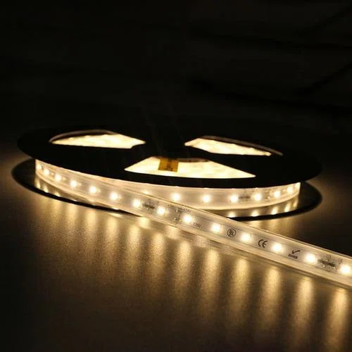
In modern electronic manufacturing, SMD LEDs (Surface Mount LEDs) have completely replaced traditional through-hole LEDs and are widely used in smart terminal indicator lights, display backlights, automotive-grade lighting, and high-power white light lighting modules.
Unlike ordinary SMD resistors and capacitors, SMD LEDs are optoelectronic devices that combine photoelectric conversion sensitivity, thermal sensitivity, and physical structural fragility. Their packages are typically made of organic epoxy resin, organic silicone, and leadframes or ceramic substrates. During PCB mounting, improper pad design, inappropriate stencil openings, excessively steep reflow soldering temperature profiles, or improper placement pressure control can easily lead to serious quality problems such as tombstoning, open circuits, adhesive peeling, reverse polarity, and accelerated light decay.
How to mount SMD LED on PCB? A deep understanding of SMD LED pin polarity identification, PCB pad DFM design, SMT batch reflow soldering processes, manual rework procedures, and typical failure modes is crucial for ensuring high product yield and long lifespan.
SMD LED Physical Packaging Structure and Polarity Identification
Before PCB design and mounting, the primary task is to accurately identify the physical pin polarity (anode and cathode) and housing structure characteristics of the SMD LED.
Common SMD LED Packaging Specifications Classification
The most commonly used SMD LED packages in the industry are mainly divided into two categories:
Small signal indicator packages (imperial dimensions): such as 0402, 0603, 0805, 1206. These LEDs are small in size and often use glass epoxy resin (FR-4) or BT resin as the substrate, with an epoxy resin lens on top, suitable for high-density onboard status indication.
Power/medium power lighting packages (metric dimensions): such as 2835, 3030, 3528, 5050, 5630. These LEDs typically contain a metal lead frame and an exposed thermal pad, with a high-transmittance silicone encapsulation on top, capable of handling drive currents from hundreds of milliamps to several amps.
Pin Polarity Identification Rules
Incorrect SMD LED polarity can cause the circuit to either fail to light up or break down in the reverse direction. Polarity identification must follow these physical markings:
Bottom Screen Markings: Most 0603/0805 packages have a green “T” or arrow pattern printed next to the bottom pad. The horizontal bar of the “T” or the tip of the arrow points to the cathode (negative terminal [-]).
Chamfer/Notch Markings: On surface mount packages such as 2835 and 3528, there is usually a physical notch at one corner of the plastic casing (PPA/PCT). The pin with the notch is the cathode.
Lead Length and Internal Structure View: For some chips with transparent colloid, viewed from top, the end with the larger physical area of the internal metal frame is usually the cathode (negative electrode).
PCB Footprint and DFM Design for Manufacturability Specifications
Pad size design directly determines the surface tension balance of the molten solder during soldering. Oversized pads or asymmetry on both sides are the root cause of poor mounting.
Pad Size and Anti-Tombstoning Balance
For small-sized dual-ended SMD LEDs such as 0603/0805, if the solder tension of the molten solder at both ends is inconsistent during reflow soldering, it will pull up one end of the component, causing a tombstoning failure.
Solder Mask Defined Pads (SMD) vs. Non-Solder Mask Defined Pads: NSMD (Non-Solder Mask Defined) pads are recommended, meaning there should be a gap of at least 2 mil between the edge of the copper foil pad and the solder mask opening. This ensures that the solder not only covers the top surface of the pad but also wets the sidewalls, providing better self-alignment.
Physical symmetry of left and right pads: The width of the conductors connecting the pads at both ends must be consistent. If one end connects to a large copper plating and the other end connects to a thin signal line, the large copper foil will dissipate heat rapidly, causing the solder melting at that end to lag, leading to tension imbalance and tombstoning. Copper plating pads must be designed with thermal relief.
Thermal Via Matrix Design for Power LEDs
For power SMD LEDs with a central independent heat sink (such as 2835/3030/3528), heat is mainly conducted vertically to the inner layers of the PCB or the bottom ground copper layer through the bottom thermal pad.
SMT Batch Mounting and Reflow Profiling Process
On SMT assembly lines, SMD LEDs are sensitive devices susceptible to damage from mechanical stress and thermal shock.
Stencil Opening Design
To prevent solder balls or the central hot pad from lifting the device and causing the leads to become suspended, the stencil openings require fine adjustment:
Small signal LED stencil openings: Typically use a 1:1 opening ratio, or finely adjust to rounded rectangles to reduce dead corners.
Central large-area hot pad meshing (Mesh/Windowing): The central hot pad opening must not be a single large opening; it must be cut into a mesh (e.g., 4 or 9 small squares), controlling the opening ratio to 65% to 75% of the total pad area. This provides an escape path for flux volatiles, reducing the void rate of the solder seam below the hot pad to below 15%.
Pick-and-place machine nozzle and placement pressure control:
Nozzle selection: For LEDs with a flexible silicone lens on top (such as a 3535 silicone convex lens), hard metal nozzles are strictly prohibited. Soft silicone or PTFE nozzles must be used. The nozzle’s inner diameter must be larger than the lens’s outer diameter. The suction position should be on the LED’s plastic housing frame. Direct pressure on the soft silicone top is strictly prohibited, as this will cause deformation and breakage of the internal gold wire.
Placement height and Z-axis pressure: The pick-and-place machine’s Z-axis depth must be precisely set. The placement pressure should be controlled between 1.5 and 2.5 Newtons (N) to prevent excessive impact from crushing the LED frame.
Reflow Temperature Profile specifications:
SMD LEDs are extremely sensitive to peak temperatures and heating rates. An inappropriate temperature profile can lead to lens peeling or yellowing of the adhesive. The following are the physical parameters for the lead-free reflow soldering temperature profile of lead-free solder paste (SAC305):
Manual Soldering and Small Batch Rework Engineering Specifications
During sample development or on-site rework phases, if batch reflow soldering is not feasible, a strict manual soldering process must be adopted.
The core logic of manual soldering SMD LEDs is: strictly control the contact temperature and time, and never allow the soldering iron tip to directly contact the LED colloid or casing.
Preparation for Protection and Anti-static Grounding: Anti-static wrist straps must be worn at all times. The light-emitting chips inside SMD LEDs (especially gallium nitride-based blue/green/white LEDs) are electrostatic sensitive devices (ESD Class 2 and above). Before operation, ensure that an anti-static mat is placed on the workbench and that the soldering iron’s metal casing is properly grounded to prevent electrostatic discharge from damaging the chip’s P-N junction.
Pad Pretreatment and Flux Application: Apply an appropriate amount of rosin-based non-cleaning flux. Clean the PCB pad surface oxides using isopropyl alcohol (IPA). Apply a thin layer of liquid flux to the pads. If manually mounting new components using a temperature-controlled soldering iron, pre-pile a small amount of solder onto one of the pads (e.g., the anode pad).
Component positioning and single-sided pre-fixation: Set the soldering iron temperature to 310°C to 330°C. Use high-precision anti-static tweezers to hold both sides of the SMD LED housing (do not grasp the top lens colloid), verifying that the pin polarity markings match the PCB silkscreen. Place the LED on the pad, heat the pre-soldered pad with the soldering iron tip to melt the solder and lock the pin in place, then remove the soldering iron.
Second-end pin soldering and fusion: Limit the heating contact time to within 3 seconds. Gently press the top of the LED housing with tweezers (keeping it aligned), and simultaneously contact the unsoldered pin and pad on the other side with the solder wire and soldering iron tip. After the solder has fully wetted the pad and the LED side, remove the solder wire first, then remove the soldering iron.
Hot Air Gun Rework and Removal (If Replacement Required): Set the hot air gun to low to medium speed and the temperature to 280℃. When reworking a faulty LED, aim the hot air gun nozzle at the pads around the LED, maintaining a distance of 1 to 2 cm for even heating. After the solder at both ends is completely melted, use tweezers to gently and vertically lift the component. Never forcibly pull the pads before the solder is completely melted to prevent PCB copper foil peeling.
Common Engineering Defects and Failure Mode Diagnosis in SMD LED Mounting
The following is an analysis of common SMD LED failure phenomena and their root causes during mounting production and subsequent operation:
Moisture Sensitivity (MSL) and “Popcorning” Effect
Physical Mechanism: The encapsulating compound (PPA/EPOXY) of SMD LEDs is hygroscopic. SMD LEDs are typically classified as MSL 3 or MSL 4 moisture-sensitive devices. If the LED is exposed to air for more than the specified limit after opening (e.g., 168 hours for MSL 3), the internal colloid will absorb a large amount of moisture. At the high temperature of reflow soldering, the water molecules vaporize instantly and expand violently, causing the encapsulation to burst, the gold wire to break, and resulting in open circuits and dead LEDs.
Engineering Solution: Check the humidity indicator card (HIC) before opening. If it is expired or has absorbed moisture, it must be baked in a vacuum oven at 60°C to 70°C for 12 to 24 hours to re-dehumidify before being put into online soldering.
Phosphor Damage and Color Shift
Physical Mechanism: White LEDs produce white light by exciting the yellow-green phosphor (YAG) on the top layer with a blue light chip. If solvents containing corrosive chemicals (such as chlorine, bromine, and sulfur) are used during the mounting or cleaning process, or if a high-pressure air gun is used to directly blow away the soft silicone, it can lead to damage to the phosphor layer or sulfidation poisoning, causing the LED’s color temperature to become severely bluish, dim, or its color rendering index to drop sharply.
Engineering Countermeasures: When cleaning mounting boards, it is strictly forbidden to use powerful ultrasonic cleaning. Neutral cleaning agents should be used, and prolonged contact between volatile sulfides (such as some rubber gaskets or inferior cardboard boxes) and the LED adhesive should be prevented.
Gold Wire Necking Caused by Hot Press Shear Force
Physical Mechanism: The LED chip and lead frame are ultrasonically bonded by micron-sized gold wires. If the pick-and-place machine nozzle depresses too deeply, or the reflow soldering cooling section cools too quickly, the shear force caused by the difference in thermal expansion coefficients between the dissimilar materials (silicone and metal frame) acts on the gold wire neck, causing the gold wire to break. This manifests as a hidden contact defect where the LED lights up when lightly pressed and goes out when released.
Engineering Countermeasures: Optimize reflow soldering cooling profiles and rigorously calibrate the SMT placement head Z-axis height and pressure sensor.
SMD LED Placement Full-Process Engineering Checklist
To ensure the placement quality of SMD LEDs on the PCB, engineers should check the following checklist before production begins:
Component Material Inspection: Confirm LED humidity sensitivity rating (MSL), check for leaks in vacuum packaging, and perform low-humidity baking if necessary.
Polarity Drawing Verification: Verify the mapping relationship between the Gerber silkscreen arrow direction and the physical pins in the component datasheet, ensuring the angle direction (0°/90°/180°/270°) in the SMT placement process is absolutely correct.
Pad Solder Mask Design: Confirm that the pads on both sides are symmetrical, thermal vias have been treated with solder mask or resin plugging, and large-area copper pours have been thermally insulated.
Stencil Thickness and Apertures: 0603/0805 recommends using a 0.12 mm (5 mil) thick stencil; the central heat dissipation pad has been meshed with openings to prevent solder overflow and short circuits.
Placement Parameter Settings: The nozzle inner diameter should avoid the top protruding lens; the downward pressure should be less than 2.5 N.
Reflow Oven Temperature Measurement: Use a thermocouple to measure the actual temperature at the LED pins, ensuring the highest peak temperature is less than or equal to 250 degrees Celsius, and the TAL (>217℃) time is less than 90 seconds.