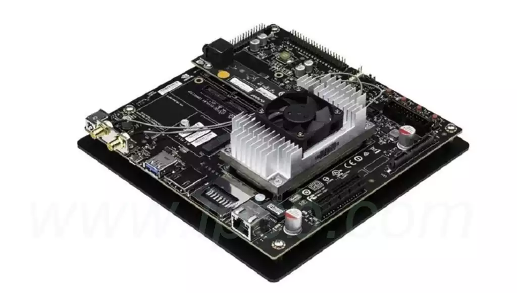
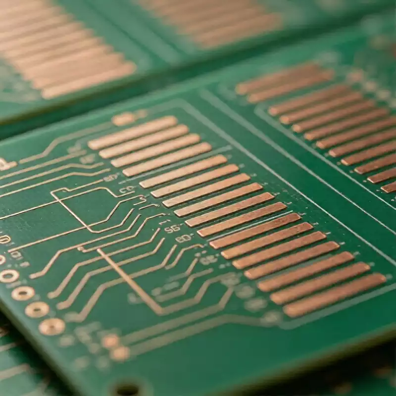
Soldering on PCB is one of the fundamental processes used to connect electronic components to a printed circuit board. By forming a solder joint between a component terminal or lead and a conductive PCB pad, the process provides both the electrical path required for circuit operation and the mechanical connection needed to keep the component securely attached to the board.
Although soldering may appear to be a relatively simple manufacturing operation, producing a reliable solder joint involves considerably more than melting solder onto a PCB. The condition of the PCB surface, component terminals, solder material, flux, pad geometry, heat transfer, and soldering method can all influence the final result. PCB design also plays an important role because copper distribution, thermal relief, via placement, and component footprints can affect how heat is transferred during assembly.
For prototype boards and repair work, components can often be soldered manually with a soldering iron. In volume production, however, SMT and through-hole components are normally processed using controlled manufacturing methods such as reflow, wave, or selective soldering. Understanding how these methods differ and how PCB design affects solderability is essential when the objective is consistent assembly quality rather than simply making an electrical connection.
What Happens During Soldering on PCB
The basic purpose of soldering is to create a metallurgical connection between the surfaces being joined. When the appropriate amount of heat is applied, the solder melts and wets the component terminal and PCB pad. Once the heat source is removed and the solder solidifies, the resulting joint provides the electrical and mechanical connection between the two surfaces.
The quality of this connection depends heavily on whether the solder has properly wetted the surfaces. Simply placing molten solder over a component lead does not guarantee a reliable joint. If the pad or component terminal is contaminated, oxidized, inadequately heated, or otherwise unsuitable for soldering, the solder may fail to spread properly.
This is one reason why professional PCB assembly treats soldering as a controlled process rather than an isolated manual operation. IPC notes that hand-soldered joints require precise technique and that improper soldering can produce defects that are not always immediately detectable through visual inspection.
Choosing the Right PCB Soldering Method
The soldering method used for a PCB depends primarily on the component technology, board design, production volume, and manufacturing requirements. Hand soldering remains useful when individual joints need to be created or modified, while automated processes are more appropriate when a board contains a large number of components that must be assembled consistently.
Hand Soldering
Hand soldering is commonly used for prototypes, engineering samples, PCB repair, rework, and relatively small production quantities. It is particularly practical when individual through-hole components or selected SMT components need to be installed or replaced.
The process relies on a soldering iron to transfer heat directly to the joint while solder wire is introduced to the heated connection. The objective is to heat both the PCB pad and the component terminal sufficiently so that the solder can wet the surfaces properly. Applying solder directly to an inadequately heated joint can result in poor wetting and an unreliable connection.
Manual soldering offers considerable flexibility, but that flexibility also introduces process variation. IPC technical material on hand soldering identifies excessive solder, insufficient solder, overheating, cold joints, contamination, and solder spikes among the common defects that can occur during manual soldering.
Reflow Soldering
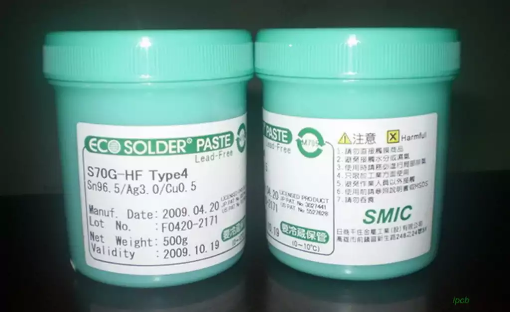
Reflow soldering is widely used for surface-mount technology because it can process many components during a single controlled heating cycle. Solder paste is deposited onto the PCB pads, the SMT components are positioned on the paste, and the assembled board is then heated according to a defined thermal profile.
During reflow, the solder particles in the paste melt and form joints between the component terminals and PCB pads. The quality of the finished assembly depends on several factors working together, including solder paste deposition, component placement, pad geometry, thermal distribution, and the reflow profile.
For densely populated SMT boards, reflow provides a level of process consistency that would be difficult to achieve by manually soldering every connection.
Wave Soldering
Wave soldering is traditionally associated with through-hole PCB assembly. Components are inserted through the PCB, and the underside of the board is brought into contact with a controlled wave of molten solder.
Because the soldering process affects a large portion of the board at once, component orientation, pad design, hole geometry, copper distribution, and board layout all need to be considered before manufacturing. Wave soldering can be highly effective for assemblies with a significant number of through-hole connections, but it is not simply a substitute for reflow soldering because SMT and through-hole assemblies have different process requirements.
Selective Soldering
Selective soldering is useful when a PCB contains through-hole components that cannot conveniently be processed through a conventional wave soldering operation. Instead of exposing the entire board to a solder wave, the process applies molten solder to selected joints.
This approach is particularly relevant to mixed-technology assemblies in which SMT components have already been assembled by reflow while certain through-hole components still require localized soldering.
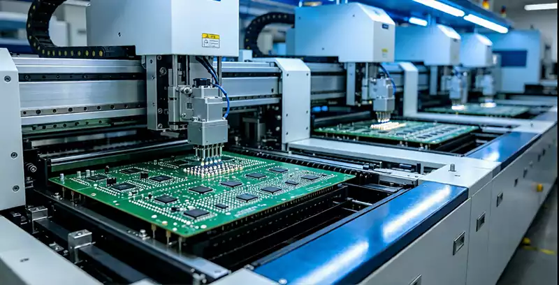
How to Soldering On PCB by Hand
When soldering a PCB manually, the quality of the final joint depends on controlling the interaction between the soldering iron, solder, PCB pad, component terminal, and flux. The process is straightforward in principle, but small differences in technique can produce noticeably different results.
Prepare the PCB Before Soldering
The PCB should be inspected before the soldering process begins. Pads and component terminals need to be free from contamination that could interfere with solder wetting, while components should be checked for correct orientation and placement.
Component orientation deserves particular attention because a solder joint can be perfectly formed while the component itself is installed incorrectly. Polarized components such as LEDs, diodes, electrolytic capacitors, and many integrated circuits have defined orientation requirements that should be verified before soldering.
PCB design can also affect the amount of heat required. A pad connected to a large copper area may dissipate heat more quickly than an isolated pad, making the joint more difficult to heat consistently.
Heat the Pad and Component Together
The soldering iron should contact the joint in a way that allows heat to reach both the PCB pad and the component terminal. The purpose is not to melt solder on the iron tip and then transfer it to the board; instead, the surfaces being joined should reach an appropriate temperature so that solder can flow and wet them properly.
This distinction becomes particularly important when a component pad is connected to a large copper plane. MIT’s PCB design material demonstrates that large copper areas can significantly affect thermal behavior during soldering, while thermal relief structures can reduce heat loss from suitable pads and make soldering easier.
Introduce the Solder to the Heated Joint
Once the pad and component terminal have reached the appropriate soldering condition, solder should be introduced to the joint. Properly heated surfaces allow the molten solder to spread across the connection rather than simply accumulating around the soldering iron tip.
The amount of solder should be controlled according to the joint geometry. Adding more solder does not automatically create a stronger connection. Excess solder can change the shape of the joint and, particularly where conductors are closely spaced, increase the possibility of bridging.
Allow the Joint to Solidify Without Movement
After enough solder has flowed into the joint, the solder feed and heat source should be removed in a controlled manner. The component and PCB connection should remain stable while the solder solidifies.
Movement during solidification can disturb the joint and affect its final structure. For this reason, stable component positioning and consistent soldering technique are important even when only a small number of connections are being produced.
Inspect the Finished Joint
Inspection should focus on whether the solder joint meets the applicable requirements rather than relying on a single visual characteristic such as surface brightness.
IPC-A-610J, published in March 2024, defines visual acceptability requirements for electronic assemblies. IPC describes J-STD-001 as the process requirement standard for soldered electrical and electronic assemblies, while IPC-A-610 provides pictorial and interpretive criteria used when evaluating completed assemblies.
For production applications, the applicable acceptance class and project-specific documentation should therefore be established before judging whether a solder joint is acceptable.
What Makes a Reliable PCB Solder Joint
A reliable solder joint is not defined simply by how much solder is present or whether the joint looks smooth. The connection needs to meet the applicable requirements for electrical continuity, mechanical integrity, solder coverage, and workmanship.
The exact appearance of a solder joint can also vary according to the solder alloy and process. Lead-free solder, for example, does not necessarily produce the same visual appearance as traditional tin-lead solder. Treating appearance alone as proof of quality can therefore lead to incorrect conclusions.
IPC-A-610J specifically distinguishes visual acceptability requirements from the processes used to manufacture the assembly, while J-STD-001 addresses materials, methods, and requirements associated with soldered electrical and electronic assemblies.
For this reason, a professional PCB assembly process should define the applicable standard, product class, inspection criteria, and manufacturing documentation rather than relying solely on informal visual judgment.
Common Problems When Soldering on PCB
Many PCB soldering problems can be traced to inadequate heat transfer, poor wetting, excessive or insufficient solder, contamination, or inconsistencies in the assembly process.
Cold Solder Joints
A cold solder joint generally occurs when the joint does not receive adequate thermal energy or the solder fails to wet the surfaces correctly. The resulting connection may have poor mechanical integrity and unreliable electrical performance.
The problem can originate from insufficient heating, poor solderability, contamination, or incorrect soldering technique. It should therefore be investigated as a process issue rather than simply corrected by adding more solder.
Solder Bridges
A solder bridge occurs when molten solder unintentionally connects two conductive areas that should remain electrically isolated. This problem becomes more challenging as pad spacing decreases because there is less physical separation between adjacent connections.
Solder bridges can be associated with excessive solder, inappropriate pad geometry, solder paste deposition problems, component placement issues, or process conditions that allow solder to remain between adjacent conductors.
Insufficient Solder
Insufficient solder can leave part of the intended connection inadequately formed. The cause may be insufficient solder deposition, poor solder feed, incomplete wetting, or an assembly condition that prevents the solder from reaching the required surfaces.
The solution is not necessarily to increase solder volume. The underlying cause needs to be identified because solder volume, pad geometry, heating, and surface condition are interconnected.
Excessive Solder
Excess solder can create its own set of problems. Besides producing an irregular joint geometry, excessive solder can contribute to bridging and may introduce undesirable stress concentrations.
IPC’s technical resource on reducing defects in hand soldering specifically identifies excessive solder as one of the common defects encountered in manual soldering operations.
Tombstoning
Tombstoning is primarily associated with small two-terminal SMT components. During reflow, one end of the component can lift away from its PCB pad, leaving the component standing at an angle.
Uneven heating and differences in solder paste deposition between the two pads are among the factors that can contribute to this behavior. PCB footprint design and thermal distribution should therefore be considered when troubleshooting repeated tombstoning defects.
Solder Voids
Solder voids are areas within a solder joint where gas or other discontinuities prevent the solder from occupying the entire intended volume. Some degree of voiding may occur depending on the process and joint structure, so the presence of a void does not automatically mean that an assembly is defective.
The significance of voiding depends on the component, joint geometry, electrical requirements, thermal requirements, and applicable acceptance criteria. Thermal pads can be particularly sensitive because the solder connection may also serve as an important thermal path.
Why PCB Design Affects Soldering
Soldering problems do not always originate in the assembly line. A PCB that has not been designed with manufacturing and thermal behavior in mind can make an otherwise controlled soldering process considerably more difficult.
Pad Geometry
The dimensions and shape of a PCB pad determine how solder interacts with the component terminal. An unsuitable footprint can create problems with solder volume, component positioning, wetting, or joint formation.
For this reason, the component footprint should be selected or designed according to the component package, PCB manufacturing capabilities, and intended assembly process.
Copper Planes and Thermal Relief
Large copper areas can draw heat away from a soldering point. When a component pad is connected directly to a substantial copper plane, more thermal energy may be required to bring the joint to the appropriate soldering condition.
Thermal relief structures address this issue by reducing the direct copper connection between the pad and surrounding copper while maintaining electrical continuity. MIT’s PCB design materials specifically describe thermal relief as a way to reduce heat transfer away from pads during soldering.
However, thermal relief should not be applied indiscriminately. MIT also notes that it can reduce the connection between a pad and the surrounding copper and may therefore be unsuitable for certain high-current or high-frequency applications.
Via Placement
Vias located near or within solder pads can affect how solder behaves during assembly. Depending on the via structure and application, molten solder can travel through a via and reduce the amount of solder remaining where it is needed.
MIT’s PCB design material notes that via size influences whether solder can wick through the via and that the interaction becomes particularly relevant to thermal pads.
This is why via-in-pad structures and thermal-pad designs often require more deliberate manufacturing considerations than conventional component pads.
Copper Distribution
The distribution of copper across a PCB can influence the thermal balance of the assembly. Two pads that appear identical in the schematic may behave differently during soldering if one is connected to a large copper region and the other is not.
This thermal imbalance can become important for small SMT components because uneven heating can affect the way solder melts and wets each side of the component.
How to Improve PCB Soldering Quality
Improving soldering quality is usually more effective when PCB design and manufacturing are considered together. A board with appropriate footprints, suitable pad structures, controlled copper distribution, and correctly positioned vias gives the assembly process a more predictable thermal and mechanical environment.
Material selection also matters. The PCB surface finish, solder alloy, flux chemistry, component finish, and storage conditions can all influence solderability. These factors should be evaluated together rather than treated as independent variables.
During manufacturing, the soldering process should be controlled according to the requirements of the specific assembly. For hand soldering, this includes controlling operator technique and rework procedures. For reflow, the solder paste printing process, component placement, and thermal profile become particularly important. Through-hole production may require wave or selective soldering parameters that are appropriate for the board’s component arrangement.
IPC’s current standards emphasize process control as part of producing consistent soldered electronic assemblies. J-STD-001 Rev J is listed by IPC as the current revision, dated April 2024.
Hand Soldering or Automated Soldering for PCB Assembly?
There is no single soldering method that is appropriate for every PCB. Hand soldering is valuable when flexibility matters more than production speed, especially for prototypes, engineering changes, repairs, and individual component replacement.
Automated soldering becomes more valuable when the board contains a large number of components or when production requires repeatable results across many assemblies. Reflow is generally associated with SMT assembly, while wave and selective soldering are used for different through-hole requirements.
The important consideration is not simply whether a particular method can create a solder joint, but whether it can produce the required joint quality consistently across the entire production run.
When PCB Soldering Should Be Part of a Complete PCBA Process
For a simple prototype, soldering may be the only assembly operation required. A production PCB assembly, however, usually involves a much broader manufacturing process.
Depending on the design, this can include solder paste printing, SMT placement, reflow soldering, through-hole insertion, wave or selective soldering, inspection, electrical testing, and controlled rework. Each stage affects the next, so soldering quality cannot always be separated from the preceding PCB design and component placement processes.
This becomes particularly important for high-density boards, fine-pitch components, thermal pads, mixed SMT and through-hole assemblies, and products with demanding reliability requirements.
IPC’s documentation makes a similar distinction between process requirements and assembly acceptability. J-STD-001 defines requirements associated with soldered electrical and electronic assemblies, while IPC-A-610 provides acceptability criteria for completed electronic assemblies.
Final Considerations for Soldering on PCB
Soldering on a PCB may appear to be a relatively simple manufacturing process, but achieving reliable solder joints is actually influenced by multiple factors, including materials, thermal conditions, component structure, PCB design, soldering techniques, and inspection standards.
For hand soldering, the key is to heat both the PCB pad and the component terminal sufficiently so that the solder can melt properly and wet the connecting surfaces effectively. At the same time, excessive heating and movement during solder solidification should be avoided. For automated assembly, greater attention needs to be paid to solder paste printing, component placement, the reflow temperature profile, PCB design, and overall process parameters.
PCB design should also be considered together with solderability rather than treated as a separate issue. Pad geometry, copper distribution, thermal relief structures, and via placement can all affect heat transfer and solder flow, ultimately influencing solder joint quality. In some cases, a soldering defect that appears to be caused by the manufacturing process may actually originate from an inappropriate PCB design.
Therefore, for professional PCB and PCBA manufacturing, reliable soldering should be treated as a comprehensive engineering and process-control issue. By considering PCB design, material selection, soldering processes, equipment parameters, and inspection standards together, manufacturers can improve process consistency, reduce soldering defects during production, and enhance the long-term reliability of the finished product. For electronic products that require stable electrical and mechanical connections, soldering on PCB is not only a fundamental assembly process but also an important factor in determining PCB assembly quality and overall product reliability.