IC packaging is a method of protecting semiconductor components from external physical damage or corrosion by encapsulating them in an encapsulating material made of ceramic or plastic. There are many different types of integrated circuits that follow different circuit designs and enclosure requirements. This translates into different types of IC package types design.
Why is IC packaging important?
Integrated circuits are often fragile and do not have connectors or pins to attach to a circuit board. By introducing a circuit package, a chip carrier is used to protect the delicate structure of the IC and provide a pin connector. This protection is made possible by the fact that the plastic, glass, metal or ceramic materials used to manufacture the package provide a physical barrier against external shock and corrosion, and IC packages have the added advantage of thermally regulating the devices in which they are used.
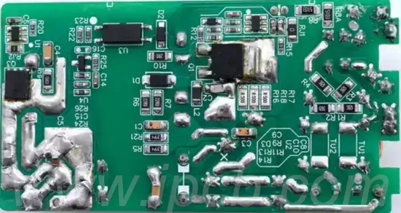
In addition, the package consists of individual components that contribute to the overall performance of the IC and ensure reliability. The leads are usually made of copper and thin tin coatings and are connected to the package with thinner wires. These are useful in creating a strong connection between the leads and the IC. Thereafter, the leads are bonded to conductive pads on the semiconductor chip and then soldered to the PCB outside the package Even discrete devices such as capacitors, transistors, or diodes are available in a variety of small pin-count packages.
IC Package Types
DIP package technology, or dual inline-pin package, is a type of IC chip packaging, also known as dual inline package or dual inline package, which is widely used especially in DRAM components. It is packaged in the form of a dual inline-pin package, which is chosen by the majority of small and medium-sized integrated circuits, and the number of pins is usually controlled within 100.
The CPU chip in DIP package has two rows of pins, which need to be precisely inserted into the socket of the matching DIP structure chip. In addition, it can also be directly soldered to a circuit board with the same number of solder holes and geometric arrangement.However,extra care is needed when inserting and removing chips in DIP packages to avoid damaging the pins.
DIP packages are available in a variety of forms, including multi-layer ceramic dual in-line DIPs, single-layer ceramic dual in-line DIPs, and leadframe DIPs (covering glass-ceramic-sealed, plastic-encapsulated structural, and ceramic-low-fusing-glass-encapsulated types, etc.).
Features.
DIP packages are very convenient for through-hole soldering on circuit board, and the operation process is relatively simple.
Due to the large ratio between the chip area and the package area, the volume of the DIP package is also relatively large.
In the early stages of IC development, CPUs such as the 4004, 8008, 8086, 8088, etc. were packaged in DIP packages, and their pins could be easily inserted into slots on the motherboard or soldered to the motherboard.
In the days when memory particles were plugged directly into the motherboard, the DIP package format was popular for its convenience. There is also an improved form of DIP packaging, known as SDIP (Shrink DIP, Shrink Dual Inline Package), which has a six times higher pin density than DIP.
However, due to the larger area and thickness of the DIP package, the pins are easily damaged during insertion and removal, making it less reliable. In addition, due to process limitations, the number of pins in a DIP package usually does not exceed 100. With the continuous improvement of CPU internal integration, the DIP package has gradually withdrawn from the stage of history. Nowadays, we can only see the shadow of DIP package on some old VGA/SVGA graphics cards or BIOS chips.
PGA packaging technology, i.e. Pin Grid Array, often referred to as Pin Grid Array, is an important packaging method in the field of integrated circuits, especially common in microprocessor packaging.
In PGA packaging, integrated circuits (ICs) are soldered to a circuit board, while the other side of the board is distributed with neatly arranged pins, which can be inserted or soldered into the corresponding sockets of other circuit boards in a specific arrangement. This design makes the PGA package especially suitable for applications that require frequent plugging and unplugging. Typically, PGA pins are spaced 1/10 inch or 2.54 mm apart, ensuring good connection stability and signal transmission efficiency.
Compared with the traditional dual-row in-line package, PGA packages usually have a smaller footprint on the same number of pins, thus improving board space utilization.
PGA packaging technology is characterized:
Its plug and play operation is more convenient, users can easily install and remove, while ensuring high reliability and reducing the risk of damage caused by improper operation.
PGA packaging technology is able to adapt to higher frequency requirements, so that the packaged IC can still maintain stable performance in high-speed operation.
BGA package, or Ball Grid Array, is a surface adhesive packaging technology applied to integrated circuits. Often used to permanently secure devices such as microprocessors, BGA packages offer higher pin capacity than traditional dual in-line packages (DIP) and quad-flat-pin packages (QFP). The entire bottom surface of the device can be used as pins, not just the edges, resulting in shorter average wire lengths and providing superior high-speed performance.
BGA package features:
It realizes high density arrangement of pins.
It has good thermal conductivity.
Low inductance pin design is adopted.
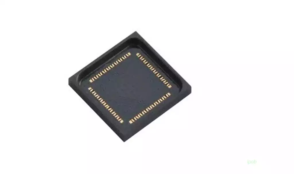
And QFP package, i.e. four side pin flat package, is a packaging technology suitable for CPU chips. This technology has a small pin pitch and extremely thin pins, and is usually used for packaging of large-scale or very large-scale integrated circuits. Its pin count often exceeds 100.
Characteristics of the QFP package:
It is ideally suited for mounting and routing on Printed Circuit Boards using SMD (Surface Mount Technology).
Suitable for high-frequency operating environments.
Easy to operate with high reliability.
The ratio between chip area and package area is small, effectively improving space utilization.
LCC package
The form of LCC package is designed for pinless chip package, this package adopts SMD package, its pins in the chip edge ground step inward bending, close to the chip, reducing the installation volume. However, the disadvantage of this chip is the use of debugging and welding are very troublesome, the general design are not directly welded to the printed circuit board, but the use of PGA package structure of the pin conversion seat welded to the printed circuit board, and then the LCC package chip installed into the pin conversion seat of the LCC structure form of mounting slots, so that the chip can be disassembled at any time to facilitate debugging.
COB package
Its full name is chip – on – board, i.e., chip-on-board packaging, is a new type of encapsulation technology different from the SMD surface-mounted encapsulation, specifically the bare chip with conductive or non-conductive adhesive adhesive on the PCB, and then lead bonding to achieve its electrical connection, and use the glue to the chip and bonding lead encapsulation.
COB package chip and related components with ASM solid crystal machine directly mounted on the printed circuit board chip and related components through the ASM wire bonding machine metal wire bonding or welding mode, can be made with the help of PCB wiring for electrical connections through the PCB wiring leads to the relevant electrodes, and covered with resin to be protected.
SO Series Packages
SO series packages cover a wide range of types including SOP (Small Outline Package), TOSP (Thin Outline Package), SSOP (Shrinking SOP), VSOP (Very Small Outline Package), and SOIC (Small Outline Integrated Circuit Package), etc. These packages are similar to QFPs. These packages are similar to the QFP, but are characterized by the chip only on both sides of the pin, showing the “L” pin layout. This type of package belongs to a surface mount package, with easy package operation, high reliability, so it has become one of the mainstream package. It is commonly used in some memory type ICs.
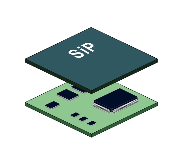
SIP Package
SIP packaging refers to the preferential assembly of multiple active electronic components with different functions, optional passive devices, and other devices such as MEMS or optical devices to form a single standard package with a specific function, which in turn constitutes a system or subsystem. From an architectural point of view, a SIP integrates multiple functional chips, such as processors, memories, etc., into a single package to realize a fundamentally complete function. Compared to SOC (System on Chip), which is a highly integrated chip product, SIP utilizes different chips side-by-side or stacked in a package.
3D Packaging
3D wafer-level packaging covers CIS emitters, MEMS packages, and standard device packages. This packaging technology refers to the realization of packaging by stacking two or more chips in the vertical direction without changing the size of the package body. It originated from the stacked packaging of flash memory (NOR/NAND) and SDRAM.The main features of 3D packaging include multi-functionality, high performance, realization of high density in large capacity, exponential increase in functions and applications per unit volume, and low cost.
Classification:
Packaging trends are moving toward stacked packages (PoP), especially those chips with low yields seem to favor PoP technology.
For high-density and high-performance chips, the multi-chip package (MCP) approach is more popular.
System-in-Package (SiP) technology is also one of the main streams, in which logic and memory devices are fabricated in their own processes and later combined in a SiP package.
Currently,most Flash memories are packaged in Multi-Chip Package (MCP) technology, where ROM and RAM are packaged together.Multi Chip Package (MCP) technology is a technology that assembles miniature components (bare chips and chip components) on a high-density multilayer interconnect substrate through a micro-soldering and encapsulation process, resulting in the manufacture of high-density, high-performance, and high-reliability microelectronic products (including assemblies, components, subsystems, and systems).
Each IC package types technology is an important milestone in the development of the electronics industry. They not only promote the progress of integrated circuit technology, but also provide a stable and reliable hardware foundation for all kinds of electronic devices. With the continuous development of science and technology, we believe that more innovative packaging technologies will be introduced in the future, bringing more possibilities and opportunities for the electronics industry.