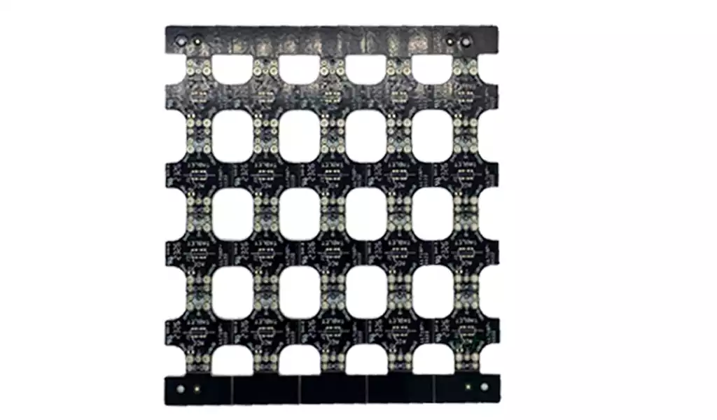
In modern electronic engineering manufacturing systems, 2 layer PCB board still hold a significant market share due to their high production cost-effectiveness, fast delivery cycles, and mature process chains. From front-end control modules in consumer smart hardware and main control boards in home appliances to sensor signal acquisition front-ends in industrial settings, 2-layer PCBs are ubiquitous. However, with the widespread adoption of high-frequency switching power supplies and the continuous increase in microcontroller clock speeds, the edge steepness of circuit signals has increased dramatically. This makes the originally simple 2-layer PCB face extremely stringent electromagnetic compatibility and signal integrity challenges.
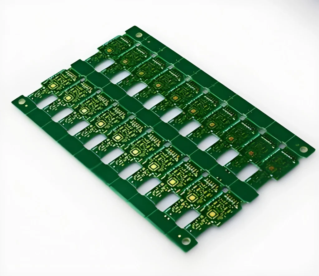
Unlike four-layer or six-layer boards with a complete inner reference ground plane, the top and bottom physical layers of a 2-layer PCB not only need to handle the majority of electrical signal routing but must also simultaneously accommodate the construction of power distribution networks and ground return paths. In the limited space of a 2-layer PCB board, even micrometer-level trace deviations and improper topology vias can instantly disrupt low-impedance return paths, leading to severe high-frequency electromagnetic radiation, ground bounce noise, and crosstalk between channels.
To build a robust 2-layer PCB board within cost-constrained physical conditions, hardware engineers must conduct a comprehensive and in-depth analysis of return paths, impedance matching, planar meshing, and noise isolation from the perspectives of microscopic electromagnetics, transmission line theory, and thermodynamics.
The Cornerstone Architecture of a 2-layer PCB Board
Many beginners mistakenly believe that current always flows back to the negative terminal of the power supply along the shortest physical path. This holds true for DC or low-frequency signals, but when dealing with AC and high-frequency signals at tens or even hundreds of megahertz, the laws of microscopic electromagnetics take precedence.
The Least Impedance Path and the Physical Accumulation of High-Frequency Return Current
In a 2-layer PCB board, the return path for AC signals or steep pulse signals is not determined by ohmic resistance, but by loop inductance. According to the principle of minimum impedance in microscopic electromagnetics, high-frequency currents always choose the path of least inductive reactance to return. The loop reactance is directly proportional to the area of the geometric loop formed between the signal line and its return conductor.
When a high-frequency signal trace is located on the top layer of a 2-layer PCB board, its generated electromagnetic field will seek the nearest reference conductor in adjacent physical space. If a continuous ground plane is laid on the bottom layer, a microscopic mirror current equal in magnitude but opposite in direction to the signal current on the top layer will be induced in the bottom layer ground copper foil. This mirror current will automatically concentrate tightly within the copper foil physical area directly below the top layer signal trace to minimize the geometric loop area between the signal line and the return line, thus reaching the lowest point of the system’s energy state.
Once the bottom layer ground copper foil of the 2-layer PCB board is cut by other intersecting traces, the mirror current must bypass the cut and be forced to take a very long, winding path. This dramatic increase in return loop area directly leads to a significant increase in parasitic inductance of the traces, generating a strong antenna radiation effect. This makes the circuit board highly susceptible to emitting high-frequency noise or being affected by external electromagnetic interference.
Single-sided Mesh Ground vs. Double-sided Cross Ground Topology
Since a 2-layer PCB board only has two copper layers, it is almost impossible to maintain a completely uninterrupted copper foil on a single layer during actual routing. To resolve this contradiction, engineers must adopt a scientific double-sided mesh ground topology strategy.
When designing a 2-layer PCB board, a priority allocation principle should be established: the top layer should primarily be defined as the horizontal signal routing layer, and the bottom layer should primarily be defined as the vertical signal routing layer and a large-area reference ground layer. All unnecessary traces should be completed on the top layer as much as possible, reserving the bottom layer for continuous copper pours to the greatest extent possible.
When the bottom layer must have vertical crossover traces, the trace length should be strictly limited, and long cut lines are strictly prohibited. After a trace passes through a multilayer PCB, it should immediately return to the top layer via a via. Grounding vias should be installed at both ends of the cut seam, and ground copper strips should be laid in the unused area of the top layer to form a three-dimensional mesh connection with the bottom ground plane. While this mesh ground network cannot compare to the complete plane of a multilayer board, it can significantly shorten the physical path of mirrored current, ensuring the stability of the high-frequency characteristics of the 2-layer PCB board.
Signal Integrity Control of 2-Layer PCB Boards
In high-speed and high-frequency circuits, traces are no longer lossless wires, but transmission line models with distributed resistance, inductance, and capacitance. Impedance control on 2-layer PCB boards is physically far more challenging than on multilayer boards.
Influence of Microstrip Line Geometry and Dielectric Layer Thickness
On a 2-layer PCB board, the top layer trace and the bottom ground plane directly beneath it constitute a typical microstrip transmission line model. The characteristic impedance of a microstrip line mainly depends on the trace width, copper foil thickness, substrate dielectric constant, and dielectric layer thickness.
The total thickness of a standard double-layer board is typically 1.6 mm. This means the dielectric distance between the top-layer signal line and the bottom-layer ground plane reaches an extremely thick 1.5 millimeters. According to the physical model for microstrip line impedance calculation, a thicker dielectric layer requires extremely wide traces to achieve a 50-ohm characteristic impedance.
On a standard 2-layer PCB board, to match a 50-ohm RF characteristic impedance, the top-layer trace width often needs to be more than 2 millimeters. Such wide traces are completely impossible to achieve around many densely pinned surface-mount chips. Therefore, when designing RF and high-speed signals on a double-layer board, a coplanar microstrip line structure is usually introduced. This involves additionally laying ground copper foil on both sides of the signal trace on the same layer, utilizing the edge capacitance effect of the same layer to lower the impedance, thereby compressing the trace width to a reasonable physical range.
Cross-Gap Tracing and Capacitive Crosstalk Suppression
In 2-layer PCB board layout design, the most taboo physical defect is a signal trace crossing a cut in the ground plane. When a high-speed signal line crosses a cut, the characteristic impedance of the transmission line will experience a precipitous drop at that point. This impedance discontinuity induces severe signal reflection, leading to severe overshoot, undershoot, and ringing at the receiver.
Besides impedance abrupt changes, cross-slot traces significantly exacerbate microscopic electromagnetic crosstalk between parallel traces. Distributed capacitance and distributed inductance exist between two closely parallel signal traces. When a level transition occurs on one trace, the changing electric field couples a capacitive current through the distributed capacitance, and the changing magnetic field induces an inductive voltage through the distributed inductance.
To minimize crosstalk on a 2-layer PCB board, the three-trace-width rule must be strictly adhered to; that is, the center-to-center distance between two parallel signal traces must be greater than or equal to three times the trace width. For strong interference sources such as clock lines and high-frequency switching lines, the center-to-center distance should be increased to more than four times, and protective ground lines should be installed on both sides of the traces to achieve physical electromagnetic shielding.
Thermodynamics and Decoupling of 2-layer PCB Boards
Due to the lack of an independent inner power plane, the power distribution network of a 2-layer PCB board can only be achieved through mesh or tree-like traces. Ensuring low DC voltage drop, high transient response, and good thermal response within a limited space is a core challenge in two-layer PCB power supply design.
Tree and Mesh Power Topologies and Star Nodes
In a two-layer PCB, it is strictly forbidden to connect all chip power pins in series with a single, thin trace like a string of pearls. This series topology causes the chip at the end of the trace to experience a huge voltage drop due to line resistance, and power supply noise generated by the preceding chips will be injected into the following chips without obstruction along the power trace.
A scientific two-layer PCB power supply topology must employ a star-shaped single-point divergence or a mesh backbone architecture. After the power supply is led out from the power management chip or main filter capacitor, a relatively wide trace should form the backbone, then branch out like tree branches to various functional modules.
For high-power devices and weak signal processing modules, the power tree must completely branch at the main capacitor to achieve physically independent power supply, preventing power sag caused by high-power device pumping from contaminating sensitive preamplifier circuitry.
Physical Geometric Placement and Microscopic Circuitry of Decoupling Capacitors
Decoupling capacitors act as miniature reservoirs, smoothing power supply noise and providing transient energy at the microsecond and nanosecond levels. On a 2-layer PCB board, the physical placement of decoupling capacitors directly determines the success or failure of their decoupling effect.
The decoupling effect of a capacitor relies on its low impedance characteristics. If the decoupling capacitor is too far from the chip’s power pins, the parasitic inductance of the connecting traces will instantly cancel out the capacitor’s high-frequency decoupling capability. Therefore, in 2-layer PCB board layout design, surface-mount decoupling capacitors must be placed close to the chip’s power pins, and the routing sequence must be that the power supply passes through the decoupling capacitor pads first, and then enters the chip pins.
Simultaneously, the ground terminal of the decoupling capacitor must be connected to the bottom primary ground plane through the shortest possible trace or an adjacent via. The loop area formed by the decoupling capacitor, the chip’s power pins, and the ground plane must be compressed to the microscopic limit, thereby sealing parasitic inductance at the nanohenry level.
Advanced 2-Layer PCB Board Physical Layer Engineering Design Red Lines
To ensure 2-layer PCB boards pass prototyping, mass production, and stringent EMC testing on the first attempt, the hardware engineering team must enforce the following six physical red lines during design checks:
Red Line 1: Bottom Layer Reference Ground Plane Integrity Red Line
The bottom layer copper area of the 2-layer PCB board must be at least 70% of the total board area. All unnecessary bottom layer traces must be removed. Any necessary vertical crossing traces must not exceed 15 mm in length, and grounding vias must be added to both sides of the cut.
Red Line 2: Critical Signal Line Insulation Crossing Red Line
All high-frequency clock lines, reset lines, high-speed communication buses, and weak analog signal lines are strictly prohibited from crossing the bottom layer ground plane cut. A 100% continuous and uninterrupted reference ground copper foil must be maintained directly beneath sensitive traces.
Red Line 3: Decoupling Loop Microscopic Geometric Area Red Line
The physical length of the trace between the chip power pin and the corresponding surface-mount decoupling capacitor must not exceed three millimeters. The closed physical loop area formed by the capacitor ground terminal and the chip ground pin must be controlled within five square millimeters.
Red Line 4: Parallel Trace Crosstalk Isolation Red Line
All switching node traces, high-frequency signal traces, and sensitive analog traces must adhere to a three-times-width spacing red line. When the length of a parallel trace exceeds twenty millimeters, a ground isolation trace must be inserted, and a ground via must be installed every five millimeters.
Red Line 5: High Current Trace Current Carrying and Temperature Rise Red Line
High current power traces on a 2-layer PCB board must be calculated based on a current carrying capacity of 1.5 amps per millimeter of trace width at one ounce of copper thickness. The solder window area of the trace must be continuous, and vias that obstruct solder flow are strictly prohibited in the window area.
Red Line Six: Electromagnetic Radiation Shielding Red Line at the Board Edge The bottom ground copper foil and the top ground copper foil must maintain a distance of more than one millimeter at the physical edge of the 2-layer PCB board, and a grounding via should be drilled every three to five millimeters around the perimeter of the board to create a Faraday cage effect and prevent high-frequency electromagnetic waves from radiating outwards from the board.