As a core component in optical communications, the stability and reliability of optical modules are paramount. The optical modules pcb design not only determines their electrical performance but also plays a decisive role in thermal management, signal protection, and manufacturability.
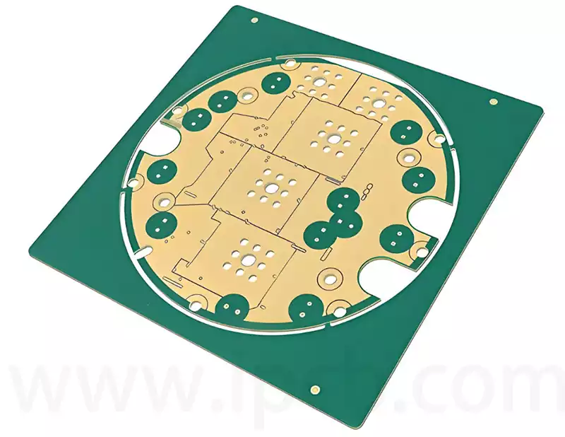
In the evolution of optical modules, PCBs predominantly adopt HDI structures—whether mechanical blind-via HDI, laser blind-via HDI, or rigid-flex + HDI. To meet standard interface dimensions, optical module PCBs typically measure 1.0±0.1 mm in thickness, with most designs comprising ≤12 layers. Two primary manufacturing processes exist for mechanical blind-via stack-ups and conventional HDI structures, as follows:
2+2: Cutting → Buried Drilling → Electroplating → Resin Hole Filling → Circuitry → Laminating → Drilling → Electroplating (some with Resin Hole Filling + CAP Electroplating) → Circuitry → Solder Resist → Marking → Surface Treatment → Forming → Testing → FQC;
4+4: Cutting → Inner layers → Laminating → Buried plating → Electroplating → Resin filling → Circuitry → Laminating → Drilling → Electroplating → (Resin filling + CAP plating for some) → Grinding and polishing → Circuitry → Solder resist → Marking → Surface treatment → Post-process.
For conventional HDI (typically 1st to 4th level HDI with 4-10 layers), the basic process is as follows:
Cutting → Drill insertion → Plating → Resin or copper paste via filling → CAP plating → Circuitry → Laminating → Laser drilling → Via filling → Circuitry (multiple cycles of laminating, laser drilling, via filling, circuitry to achieve layer increase) → Laminating → Laser drilling → Mechanical drilling → Via filling → Grinding and polishing → Circuitry → Solder resist → Text printing → Surface treatment → Post-process;
Additionally, variations in gold finger design and thermal management approaches result in differing manufacturing processes for optical module PCBs. Embedded copper blocks, copper paste filling, and through-hole filling all address optical module heat dissipation, though their implementation methods differ. Current mainstream optical modules feature either short/long gold fingers or tiered gold fingers. Printed plug fabrication involves five pattern transfers: outer layer circuitry once, solder resist exposure once, printed plug plating once, lead etching once, and selective gold plating or nickel-palladium plating once.
Optical modules impose stringent thermal management requirements, with heat sources primarily concentrated around chips and optical components (such as TOSAs and ROSAs). Typically, thermal management in optical modules is achieved through three approaches: power reduction, efficient heat conduction, and rational layout. Reducing power consumption aims to minimise heat generation; efficient thermal conduction rapidly dissipates heat to prevent accumulation and adverse effects; rational layout employs specific measures to isolate heat-sensitive components from heat sources when effective dissipation is unattainable.
Given the extremely confined internal space of optical modules, strong convection cooling is impractical, necessitating reliance on thermal conduction for heat dissipation. Thermal conduction can be further categorised into external and internal conduction. Internal conduction is primarily addressed through the encapsulation materials of optical components and the PCB materials. With continuous advancements in chip technology, overall power consumption has been significantly reduced. Current thermal management optimisation for optical modules focuses on enhancing thermal conductivity, expanding heat dissipation surface area, reducing contact surface roughness, improving contact surface flatness, and minimising the thickness of heat transfer paths.
On the motherboard, the primary challenge in chip cooling arises when high-heat-generating components are positioned at the bottom, whether in a daughterboard-motherboard configuration or a single-board structure. This placement hinders the rapid conduction of heat generated by the chip to the primary heat dissipation surface. Consequently, resolving thermal management in optical modules necessitates meeting specific requirements in both thermal conduction and heat dissipation.
For thermal management at the chip location within optical modules, flexible and compressible high-thermal-conductivity materials, such as thermal silicone sheets, are typically employed. These materials are highly suitable for optical module thermal solutions due to their high thermal conductivity, low pressure deflection, and low contact resistance. Thermal conductivity coefficients of common heat dissipation materials are as follows: Heat dissipation for optical module PCBs is largely achieved through material technology. Copper, owing to its high thermal conductivity, relatively low cost, and excellent compatibility with PCBs, is the preferred material for PCB heat dissipation in optical modules. Specifically, pure copper exhibits a thermal conductivity of up to 400 W/mK, while electroplated copper typically approaches 350 W/mK. Copper paste, containing higher resin content, generally ranges between 8–10 W/mK.

PCB thermal management leverages copper’s inherent properties. Common techniques include copper paste via filling, embedded copper blocks, plated-through holes, or designing PCBs as ELICs (Electrolytic-Laminated Interconnect Circuit) by stacking blind vias into columnar structures for heat dissipation.
(1) For optical module PCBs with buried copper blocks, PP and substrate windows are opened at corresponding layers. During lamination, copper blocks are embedded into the PCB. Inner-layer blocks are typically regular circular or square copper, while outer-layer blocks are generally “T”-shaped. These blocks are usually positioned beneath TOSA and ROSA chips to assist chip heat dissipation. When embedding copper blocks, dense laser-drilled blind vias are filled to rapidly conduct heat away. Due to the compact size of optical modules and the small footprint of optoelectronic conversion chips, the required module dimensions are minimal. Embedding such small copper blocks during lamination is prone to shifting, complicating the process and reducing efficiency. Additionally, misalignment of the copper block relative to its intended position can impair the flow and filling effect of the prepreg during lamination, ultimately resulting in poor thermal stress performance. Furthermore, in copper block embedding designs, the corresponding outer layers are typically substrate materials. During lamination, the browned surface of the substrate can easily adhere to prepreg dust particles. Post-lamination, prepreg residue may remain on the copper surface, ultimately affecting the optical module’s cosmetic yield rate.
(2) Copper paste filling is another major approach to address heat dissipation. Copper paste materials have evolved significantly over many years and currently offer lower cost, superior processability, and better reliability compared to embedded copper blocks. While its thermal conductivity is considerably lower than that of embedded copper blocks, the primary bottleneck for PCB heat dissipation lies in the resin. Copper paste filling achieves thermal conductivity exceeding 8 W/m·K. Copper paste via filling is generally recommended. The process resembles vacuum resin via filling, and copper paste application does not impact lamination production capacity, making it more conducive to industrialization than embedded copper blocks.
(3) Based on design economics, if the optical module itself is designed as an ELIC (Electrolytic Copper-in-Layer), large copper areas can be placed at the chip location on the PCB. Each layer is then connected via blind vias. The ELIC structure spatially emulates solid copper pillars, with the large copper surface forming vertical heat dissipation channels through these pillars. This design is costly and time-consuming to manufacture. It is generally not recommended unless extremely high routing density necessitates ELIC design for the PCB, in which case similar ELIC structures can be employed in heat dissipation zones.
(4) Via-Filling Heat Dissipation: Originating in the semiconductor electroplating industry, this technique was later adapted for PCBs requiring high thermal dissipation and reliability. Compared to semiconductor laser micro-blind vias or laser X-through-plating, X-vias typically feature an aspect ratio around 2:1. Due to a small funnel-shaped aperture at the via center, copper plating readily deposits at this location with additive assistance, closing the aperture to form upper and lower blind vias. Subsequent plating after blind via formation follows the same process as blind via filling.
The mechanism for filling through-holes is largely identical to that for filling blind holes: inhibiting plating deposition on the surface layer (high-potential region) while promoting deposition in the low-potential region to achieve filling. The low-potential region of a through-hole corresponds to its central interior. Typically, through-hole filling copper plating solutions contain more inhibitors than promoters. Since the additive concentration on the substrate surface layer is higher than inside the through-hole, this principle causes plating to preferentially deposit from the central region (low-potential area) within the through-hole. If plating deposits preferentially occur at the central region within the through-hole, the plated surfaces extending from the hole center will meet and form contact, creating two blind holes on the upper and lower surfaces of the through-hole. This phenomenon is known as electroplating bridging. Subsequently, blind holes are filled under conditions of high current density and high CuSO₄ concentration. The primary drawback of through-hole filling is its stringent parameter requirements and extremely low efficiency, typically requiring 6 to 8 hours or longer to complete.
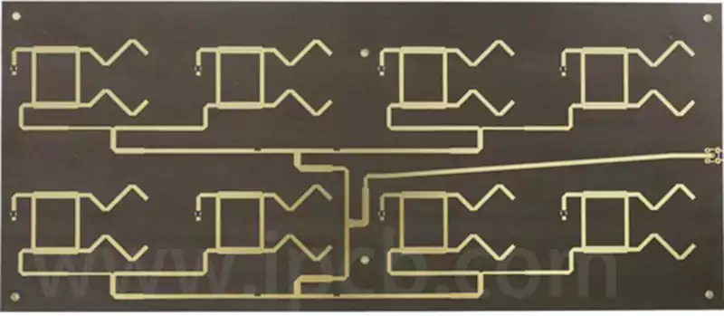
Optical port signals are weak signals requiring special protection. When routing, adhere to the following guidelines:
Separate signal traces for the receiving and transmitting ends to minimize interference. Place as many GND vias as possible around signal traces, and isolate different signals from each other.
Single-ended signals are weak, so traces should be as wide as possible (ideally matching the width of the connected pad) and kept as short as possible. When the signal width differs from the connected pad size, ensure smooth transitions in the connection. Maintain impedance matching and avoid vias in the trace layout whenever possible. If vias are necessary, pay close attention to their proper handling.
Differential signals should be kept as short and thick as possible:
The power supply voltage for lasers tends to be relatively high, requiring careful consideration during routing.
Properly manage power and GND connections.
In PCB design for optical interfaces, special attention must be paid to protecting weak signals through proper layout and routing to ensure signal quality and stability. Simultaneously, adequate thermal management and voltage routing must be implemented.
PCB design for manufacturability (DFM) for optical interfaces involves anticipating and resolving potential manufacturing issues during the design phase to ensure product quality and production efficiency. Below are DFM recommendations specific to optical interfaces.
Hole Size Issues
Hole sizes must be consistent and uniform, as variations affect drilling precision and board reliability. If holes are to be plated-through, ensure they are sufficiently large during design to guarantee adequate copper plating coverage.
Module Layout
Module placement is a critical consideration in optical port PCB design. Positioning and angular accuracy must be maintained to ensure signal integrity. Additionally, module layout must account for manufacturing precision and manufacturability.
Pad Design
Pads are a critical component in PCB manufacturing, requiring design considerations for both manufacturing accuracy and board reliability. For optical port pads, precise size and positioning are essential to guarantee signal integrity. Simultaneously, pad design must integrate with overall board layout and routing to ensure manufacturability during production.
Designing an optical module PCB involves a complex process that comprehensively balances electrical performance, thermal management, signal integrity, and manufacturability. By strategically selecting HDI structures, optimizing thermal solutions, adhering to signal routing standards, and prioritizing design for manufacturability, the stability of optical module performance and production efficiency can be significantly enhanced. During actual design, strategies should be flexibly adjusted based on specific requirements and conditions to achieve optimal performance of the optical module PCB.