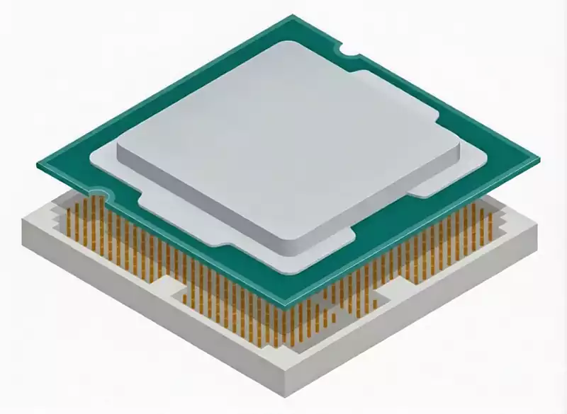
As electronic products evolve towards higher integration and miniaturisation, Ball Grid Array (BGA) packaging has become an indispensable component type in modern PCB design, thanks to its high-density interconnections and excellent electrical and thermal performance. However, the pad design, routing planning and reliability verification of BGA packaging directly determine the manufacturing yield and long-term stability of the entire product.
BGA Pad Design
1.Pad Dimensions
The pad diameter must be appropriately matched to the BGA ball diameter. Typically, the pad diameter is designed to be 10% to 20% smaller than the corresponding ball diameter. This ensures that during the soldering process, the molten solder can fully wet the pad surface, forming uniform and secure solder joints, whilst preventing excessive solder overflow that could cause short circuits between adjacent pads. For example, when the BGA ball diameter is 0.5 mm, the pad diameter can be set to approximately 0.4 mm, which meets soldering quality requirements whilst remaining compatible with standard PCB manufacturing processes.
2.Pad Shape
Common BGA pad shapes include circular and square, each with its own suitable applications; the choice should be based on actual design requirements.
Circular pads: The most widely used type, their greatest advantage lies in the reduced difficulty of aligning the solder ball with the pad during soldering, effectively mitigating the adverse effects of placement deviations.
Square pads: More suitable for high-density routing scenarios. When pin pitches are small, square pads allow for more efficient use of PCB space, increasing routing density and preventing routing congestion.
3.Pad Types (Solder Mask Design)
Based on the design of the solder mask layer, BGA pads are classified into solder mask-defined pads (SMD Pads) and non-solder mask-defined pads (NSMD Pads), each with distinct characteristics in terms of structure, performance and cost.
Solder Mask-Defined Pads (SMD Pads): The opening size of the solder mask layer is smaller than the size of the copper pad, with the soldering area determined by the opening in the solder mask layer. The advantage of this approach is that it enhances the adhesion between the copper layer pad and the PCB substrate, reducing the risk of pad detachment, whilst also offering lower manufacturing costs.
However, under long-term use (such as in harsh environments involving high-low temperature cycling or vibration), its soldering reliability is slightly lower than that of non-solder mask defined pads, making it suitable for general electronic equipment where long-term reliability requirements are not particularly high.
Non-Solder Mask Defined Pads (NSMD Pads): The soldering area is defined directly by the copper layer pad itself; the solder mask serves only an insulating and protective function and does not participate in defining the pad. Its core advantage is greater soldering reliability, with better solder joint stability under harsh operating conditions (such as in industrial equipment, automotive electronics, and aerospace applications), making it suitable for fields with high reliability requirements.
BGA Routing Design
1.Routing Layer Planning
Due to the high pin count and density of BGA packages, single- or double-layer PCBs are often unable to meet routing requirements; therefore, a multi-layer board design is generally required, typically comprising 4 or 6 layers. For BGA components with extremely high pin density, 8 layers or more may even be necessary.
When planning routing layers, signal layers should be separated from power and ground layers to prevent power supply noise from interfering with high-speed signals. At the same time, reference planes should be appropriately configured to ensure signal transmission integrity. For example, placing the power layer adjacent to the ground layer creates coupling capacitance, which reduces power supply noise and provides a stable reference environment for the signals.
2.Trace Width and Spacing
Trace width must be determined in conjunction with the magnitude of the current being transmitted and impedance matching requirements:
Power traces: These should be appropriately widened according to the current magnitude to prevent overheating or even burnout caused by excessive current.
Signal traces (particularly high-speed signal lines): Trace widths must be designed strictly in accordance with impedance requirements to ensure impedance matching and minimise signal reflection and attenuation. It is recommended to use differential pairs for high-speed signal lines, maintaining consistent spacing and equal lengths between the differential pairs to enhance signal integrity and reduce external interference.
The spacing between all traces must meet the minimum requirements of the PCB manufacturing process to avoid the risk of short circuits caused by insufficient spacing.
3.Via Design
In BGA routing, due to high pin density, a large number of vias are often required to connect signals between different layers. Via types include through-holes, blind vias and buried vias, and the choice should be based on a comprehensive assessment of the number of PCB layers, routing density and cost.
Through-holes: These pass through the entire PCB; they are simple to manufacture and low-cost, but occupy a significant amount of routing space and may have some impact on signal integrity.
Blind Vias: These penetrate only a portion of the layers (e.g., the top layer and an inner layer). They effectively save space and minimise interference with other traces, making them suitable for interconnections between the top and inner layers of multilayer boards.
Buried Vias: Located within the inner layers of the PCB without penetrating the top layer, these maximise routing density. However, their manufacturing process is complex and costly.
Regardless of the type of via selected, its dimensions must meet the minimum requirements of the PCB manufacturing process, and the design should be optimised as much as possible to minimise parasitic inductance and capacitance, thereby reducing adverse effects on signal integrity.
Design Verification and Thermal Management
1.Electrical Performance Testing
Electrical performance testing is central to design verification and primarily comprises signal integrity testing and power integrity testing.
Signal Integrity Testing: This detects issues such as reflection, attenuation and crosstalk during the transmission of high-speed signals, ensuring signal accuracy and stability, and preventing equipment malfunctions caused by distortion.
Power Integrity Testing: This assesses indicators such as power supply voltage stability, ripple and noise, ensuring a stable and clean power supply to BGA devices and other circuits, and preventing power supply noise from interfering with signals.
2.Thermal Performance Testing
BGA packages generate heat during operation. If the thermal management design is inadequate, heat accumulation can lead to excessive component temperatures, affecting performance and lifespan; in severe cases, this may cause solder joint detachment or component burnout. Therefore, thermal performance testing is essential.
Thermal imaging cameras are typically used to detect the temperature distribution of the BGA during operation and to evaluate the effectiveness of the thermal management design. If localised overheating is detected, the thermal management structure should be optimised promptly, for example by adding heat spreader pads, arranging heat-dissipating vias or fitting heat sinks.
3.Mechanical Performance Testing
The mechanical reliability of BGA solder joints directly determines the service life of PCB products under harsh conditions such as vibration and shock, which is particularly critical in sectors such as automotive electronics and industrial control. Mechanical performance testing typically includes:
Vibration testing: Simulates continuous vibration environments encountered in actual operation to detect whether solder joints exhibit fatigue failure.
Impact testing: Simulates sudden impact loads to verify the impact resistance of solder joints.
The design of BGA pads and routing is a systematic engineering process involving the selection of pad dimensions and shapes, trade-offs in solder mask definition, the planning of multi-layer routing strategies, and the appropriate use of vias. Furthermore, the electrical, thermal, and mechanical performance tests conducted during the design verification phase serve as a critical safeguard to ensure product stability from prototyping through to mass production.