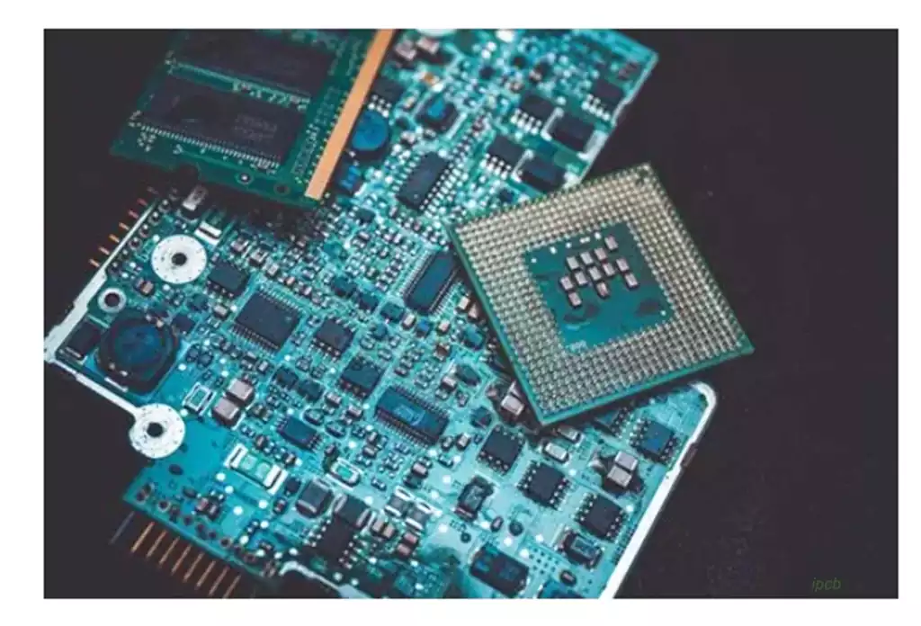
PCB jumper refers to spaces reserved on a printed circuit board for connecting circuits, achieved by adding conductive wires and connectors. They serve a broad purpose in circuit design, effectively resolving layout and routing challenges.
Jumpers serve as ‘circuit shortcuts’ in PCB design, achieved through thickened conductors or special connection methods, specifically addressing the following issues:
- Components that cannot be directly connected;
- Components positioned too far apart;
- Incorrect pin numbering requiring correction.
The Core Functions of PCB Jumper
Compensating for Design Deficiencies: In complex PCB layouts, jumpers can temporarily substitute for unrouted traces, saving both cost and time.
Circuit Repair and Optimisation: Repairing broken or damaged circuits, or activating manufacturer-disabled functional modules.
Debugging and Prototype Testing: Temporarily connecting test points during development to verify circuit functionality.
Classification and Characteristics of PCB Jumper
Fixed Jumper
Fixed jumper refers to conductive traces permanently connecting two points on a PCB board. Typically fabricated from copper or alloy materials through etching into the board, they provide stable connections requiring no subsequent modification or removal. The primary advantages of fixed jumpers lie in their low resistance characteristics and stable current-carrying capacity.
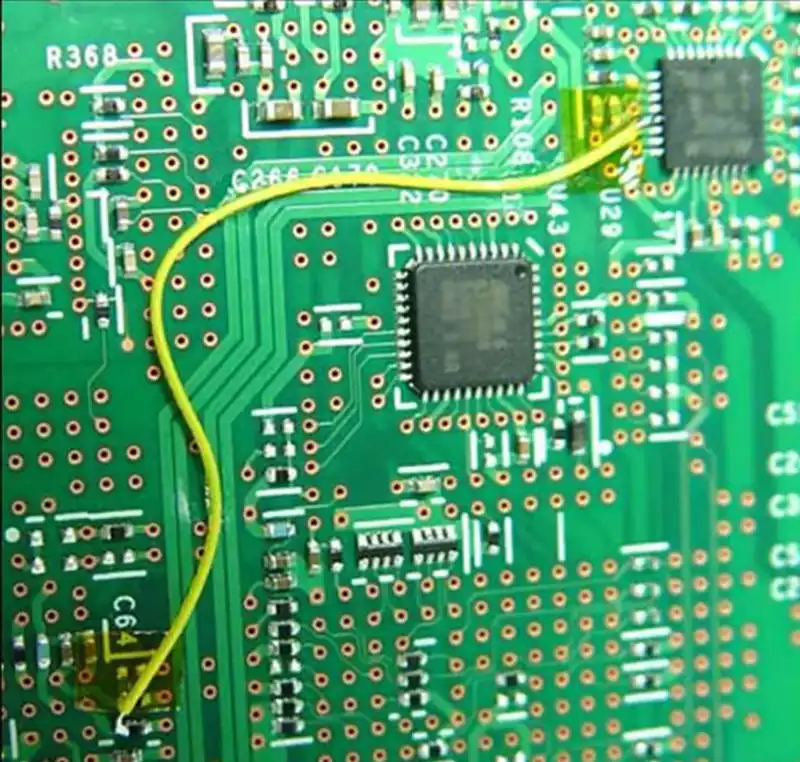
Removable Jumpers
Removable jumpers, also known as jumper caps or jumper pins, are primarily used on circuit boards requiring field configuration or debugging. Users can alter circuit connection states by inserting or removing jumper caps, offering high flexibility. Due to their removable nature, removable jumpers are more prone to faults such as poor contact compared to fixed jumpers.
Electrical Characteristics and Applications
In electronic engineering, the electrical characteristics of jumpers include resistance, capacitance, and inductance. Resistance affects signal attenuation, capacitance influences frequency response, and inductance impacts current flow. These properties determine the optimal application range of jumpers within circuits. For instance, low-inductance jumpers are required for high-frequency signal transmission to minimise signal distortion.
The production of PCB jumpers requires the following steps:
- Within PCB design software, first determine the location and length of the jumpers to be added.
- Open conductor channels on the PCB board and establish the direction and length of the jumpers.
- Install sockets at both ends of the jumpers to connect different circuits.
- Proceed with PCB manufacturing processes including printing, drilling, and component placement.
- Connect the jumpers to the board via soldering.
The utilisation of PCB jumper is critical to circuit board performance. Consequently, specific considerations must be observed during design and implementation to ensure stable circuit operation and reliability.
Jumper Length and Placement
Jumper length and layout constitute key considerations in PCB design. To prevent adverse effects on circuit functionality, jumpers must neither be excessively long nor too short. Typically, jumpers are designed in predefined length increments, such as 0.1-inch (100-mil) steps. For instance, bare conductor jumpers must not exceed 12.7 millimetres (0.50 inches) in length, measured between terminations. Jumpers may span connection pads, but sufficient clearance must be maintained to permit removal from pads when component replacement is required. During routing, avoid passing traces through narrow passages that could impede current flow, and endeavour to keep traces as short and direct as possible. Input and output traces should avoid running parallel adjacent to one another; where necessary, ground planes may be employed for isolation. To ensure no digital signal traces lie above analogue sections and no analogue traces lie above digital sections across all layers, jumpers or 0-ohm resistors may be used to connect partitioned grounds. Furthermore, jumpers should be positioned on the circuit board away from sensitive signals, such as high-frequency or analogue circuits.
Wire Gauge and Material Selection
The gauge and material selection of jumpers are critical for ensuring excellent conductivity and reliability. Tin-plated iron wire jumpers represent a common choice. Utilising iron wire as the base material with a tin coating, they offer superior conductivity and oxidation resistance while being stiffer and easier to shape than pure copper wire. Tinned iron wire with a 0.6mm diameter is recommended, available in various span specifications (e.g., 4mm to 25mm) to accommodate most standard PCB pad pitches (multiples of 2.54mm). Solid insulated copper wire is also recommended, with a suggested gauge of 22 to 32 AWG. Suitable insulation materials include Kynar, Milene, Kapton, or Teflon. Jumps on circuit boards typically employ tin-plated copper material, which offers high solderability, excellent soldering properties, lead-free environmental compliance, moisture resistance, and suitability for long-term storage.
Manufacturing and Operational Considerations
During PCB jumper production, meticulous handling is paramount to ensuring functional end products. Jumper lengths and connection methods should be kept as concise and straightforward as possible, avoiding excessive length or coiling. Pin spacing for axial components and jumpers should be maintained as uniformly as feasible to minimise component moulding and tooling requirements. When routing, allow extra width, particularly for power lines. For safety, minimise the use of vias and jumpers. Pay particular attention to soldering quality and strength, as well as interference and impact on other circuits. In switching power supply designs, jumpers may be employed to resolve cross-circuit issues, thereby simplifying the design. During jumper fabrication, first determine their positions and lengths within PCB design software. Subsequently, open conductor channels on the PCB board and establish the jumpers’ direction and length. Finally, install sockets at both ends of the jumper to connect different circuits. Proceed with PCB printing, drilling, component placement, and other fabrication processes, culminating in soldering the jumper to the board. It is crucial that both pads on the jumper are assigned identical, non-zero jumper ID values.
PCB jumper, as a flexible circuit connection method, play a vital role in compensating for design flaws, circuit repair and optimisation, and debugging and testing.