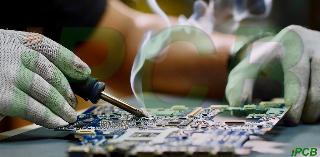
FPC has gained increasing application in the trend towards miniaturisation and portability of electronic devices, owing to their unique flexibility. However, FPC design is complex and specialised, involving multiple critical stages such as material selection, routing design, process adaptation, thermal design, and reliability-oriented design. Each stage presents numerous key considerations and potential pitfalls, requiring precise control to ensure FPC performance and reliability meet specifications.
Material Selection
The flexibility and reliability of FPCs are determined at the material selection stage. Unlike rigid PCBs, which primarily utilise FR-4 substrates, the material composition of FPCs (substrate, copper foil, cover film, adhesive) directly dictates their bending endurance, temperature resistance, and signal stability. Precise adaptation to specific application scenarios is essential—this constitutes the first critical aspect of FPC design and the stage where errors most commonly occur.
As the foundational layer of FPCs, substrate selection hinges on achieving ‘flexibility adaptation + application alignment’ rather than blindly pursuing high-end solutions. The prevailing FPC substrates in the market are polyimide (PI) and polyester (PET), exhibiting markedly distinct properties suited to entirely different scenarios: PI substrates offer a broad temperature tolerance (-200°C to 300°C), exceptional bend resistance, low moisture absorption (merely 1.5% at 85°C/85% RH), and stable insulation properties, making them the preferred choice for mid-to-high-end FPCs (e.g., foldable displays, automotive electronics, medical devices). However, PI substrates carry a higher cost. Applying them to ordinary consumer electronics (such as basic smart wristbands or simple sensors) would constitute a waste of resources. PET substrates are inexpensive and highly flexible, but they exhibit poor temperature resistance (long-term operating temperature not exceeding 120°C) and a short bending endurance life. They are only suitable for simple FPC applications involving static installation, no high temperatures, and infrequent bending (such as standard remote controls or small toys). Many designers fall into the misconception that ‘PI is superior to PET,’ blindly selecting PI substrates which leads to cost escalation, thereby contradicting the cost-effectiveness principle of FPC design.
As the ‘conductive core’ of FPC, copper foil selection directly impacts bending lifespan and signal transmission efficiency – a critical detail distinguishing FPC design from rigid PCBs. Common FPC copper foils comprise rolled annealed copper (RA) and electrolytic copper (ED), exhibiting vastly different bending properties: – Rolled annealed copper features fine grain size (<3μm), achieving dynamic bend life (per IPC-TM-650 standard) up to 150,000 cycles. It suits high-frequency bending applications (e.g., foldable screen hinges, wearable device bending zones). Electrolytic copper features coarse grains (size >5μm), with a bending lifespan only 40% that of rolled copper. However, its lower cost makes it suitable for static installations or low-frequency bending applications (e.g., camera module FPCs). Furthermore, copper foil thickness requires precise control: a thickness of 12μm to 18μm is recommended for bending zones. Excessive thickness reduces FPC flexibility, increasing the risk of copper foil fracture during bending; conversely, insufficient thickness elevates signal transmission resistance, compromises conductivity, and diminishes damage resistance.
As the protective barrier for FPCs, the selection of cover films and adhesives must be highly compatible with the substrate and copper foil to prevent delamination or lifting issues. The primary function of the cover film is to shield the copper foil and provide insulation against moisture. It must be selected from the same material family as the substrate (e.g., PI substrate paired with PI cover film, PET substrate paired with PET cover film) to ensure tight adhesion after thermal lamination. Additionally, the cover film thickness should be controlled between 25μm and 50μm. Excessive thickness increases the overall FPC profile, compromising its slim profile, while insufficient thickness fails to provide adequate protection. Adhesive selection must prioritise curing parameters and peel strength, favouring epoxy resins that meet 180°C/1.5MPa lamination specifications. Insufficient curing yields interlayer peel strength <0.8N/mm, predisposing the bond to delamination under thermal shock. Furthermore, the adhesive’s temperature resistance and moisture resistance must align with the application environment. High-end scenarios such as automotive and medical applications require adhesives with high-temperature resistance and low water absorption to prevent ageing and failure during prolonged use.
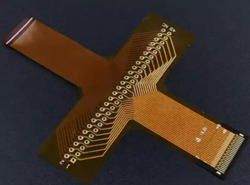
Routing Design
Routing design constitutes the very essence of FPC design and represents the most significant departure from rigid PCB design. While rigid PCB routing prioritises signal integrity and compact layout, FPC routing must simultaneously address signal transmission and, crucially, resolve stress concentration issues in bend zones. Over 60% of copper foil cracking failures in FPCs stem from suboptimal routing design. Consequently, FPC routing must adhere to the core principles of ‘minimising stress, avoiding concentration, and reserving space’, breaking away from rigid PCB design conventions.
Routing within bend zones represents the core challenge of FPC routing and is the most frequently overlooked critical aspect. Firstly, trace orientation must be parallel to the bending axis, which is crucial for preventing copper foil fracture during flexing: when an FPC bends, traces parallel to the axis ‘bend without stretching’, whereas those perpendicular to the axis repeatedly endure tensile and compressive stresses (each bend can cause 5%-10% elongation). Prolonged cycling leads to copper foil fatigue fracture. Specification requirements: All traces within the bending zone must run parallel to the bend axis, with deviations ≤5°. Perpendicular routing is strictly prohibited. Where layout constraints necessitate perpendicular traces, serpentine routing must be employed. The serpentine bend radius must be ≥0.5mm, with a stretch rate ≤3%. This serpentine structure absorbs tensile stress, extending bend life by over fivefold. In the initial design of a smartwatch FPC, three core traces were routed perpendicular to the bending axis. All traces fractured after merely 50,000 cycles. Upon adjusting to parallel routing, the bending endurance surged to 150,000 cycles, fully meeting end-user requirements.
Trace width and spacing must balance conductivity, bendability, and insulation properties, and cannot adhere to rigid PCB routing standards. Copper foil width in bend zones is recommended ≥0.2mm (0.1mm thick foil at 0.2mm width can carry 1A current, with current density controlled within the safe limit of 5A/mm²). Where installation space is constrained, the minimum width should not fall below 0.15mm, with current carrying capacity reduced (≤0.5A). Reinforcing copper strips (0.1mm wide, spaced 0.1mm from traces) should be added on both sides of the copper foil to prevent stress concentration. Excessively narrow copper foil widths (<0.15mm) present two risks: firstly, excessive current density accelerates copper foil ageing through heat generation; Secondly, reduced bending resistance leading to fracture. In a wireless earphone FPC, a 0.12mm-wide trace in the bending zone, carrying 0.8A current, failed after 30,000 bends. When widened to 0.2mm, the same 0.8A current withstood 100,000 bends without failure.
Designing trace spacing must account for substrate deformation during bending to prevent short-circuit risks. When an FPC bends, the substrate undergoes slight stretching and deformation. Excessively narrow trace spacing (<0.15mm) increases the likelihood of adjacent traces contacting and short-circuiting, particularly in high-frequency bending scenarios (e.g., 10 times per minute), where the short-circuit risk escalates significantly. Specification requirements: Trace spacing in bending zones must be ≥0.2mm, twice as stringent as non-bending zones (≥0.1mm). For high-voltage traces (≥50V), spacing must be ≥0.3mm to prevent breakdown short circuits. An automotive FPC with 0.15mm line spacing in the bending zone exhibited two short circuits after 80,000 bends. Adjusting to 0.2mm spacing resulted in no short circuits after 120,000 bends.
Additionally, two critical details must be observed for routing in bending zones: Firstly, avoid dense line placement. Maintain a line density ≤ 1 line per millimetre, with a minimum 0.3mm blank area (substrate only, no copper foil) between every two lines to serve as stress relief channels. Failure to do so increases local substrate rigidity, prevents stress dispersion, and may cause batch line fractures. Secondly, avoid large-area copper plating in bending zones. Copper foil exhibits over 50 times the rigidity of PI substrate. Extensive copper plating increases substrate stiffness, potentially causing delamination between substrate and foil or foil cracking during bending. For local reinforcement, apply 25μm-thick PI flexible reinforcement sheets instead of copper plating.
Signal integrity routing constitutes another critical aspect of FPC design. The dielectric constant (Dk≈3.5) of FPC flexible substrates exhibits significant variation, substantially exceeding that of rigid PCB FR4 substrates (Dk=4.2-4.5), presenting challenges for high-frequency signal routing. Designers must measure substrate dielectric constants in practice, optimise transmission line structures, prioritise microstrip configurations, and avoid striplines due to impedance mismatch caused by lamination misalignment. High-frequency signal traces should be kept as short and straight as possible, minimising bends to prevent signal attenuation and increased interference. Differential signal traces must maintain equal length, parallel alignment, and uniform spacing to reduce crosstalk between pairs and ensure stable signal transmission.
FPC design constitutes a systematic engineering endeavour, wherein each stage is intrinsically interconnected and indispensable. Only through comprehensive and meticulous consideration of these critical aspects can one devise high-performance, highly reliable FPCs capable of meeting the demands of diverse and complex application scenarios.