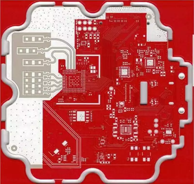
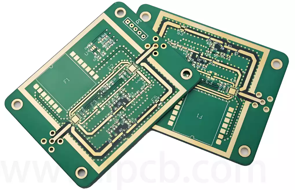
PCB High Frequency Board (RF Microwave PCB) is a special type of circuit boards used to process signals at higher electromagnetic frequencies. This type of board is commonly used in high frequency (frequencies greater than 300MHz or wavelengths less than 1 metre) and microwave (frequencies greater than 3GHz or wavelengths less than 0.1 metre) applications, and may be manufactured using normal rigid circuit board manufacturing methods or with special treatments. In general, we can define PCB high frequency boards (microwave RF circuit boards) as circuit boards above 1GHz.
RF microwave PCB is mainly used in wireless communications, radar, satellite navigation and other fields. In the field of wireless communications, microwave RF circuit boards are widely used in mobile phones, wireless LANs, base stations and other equipment to achieve high-speed data transmission and stable communications. In the field of radar, microwave RF circuit boards can be used to detect and track targets with high precision and reliability. In the field of satellite navigation, microwave RF circuit boards can be used to achieve satellite positioning and navigation functions, for aviation, space, marine and other fields have important application value.
RF microwave PCB shows significant advantages in a number of aspects, making them an indispensable part of modern electronic equipment:
High-frequency operation capability: microwave RF circuit boards are able to work stably at frequencies above 1 GHz. This enables them to achieve fast data transmission and precise signal processing, meeting the need for high speeds in modern communications. For example, the millimetre-wave frequency band is typically defined as 30 GHz to 300 GHz, and in automotive millimetre-wave radar systems, frequencies can even start at 24 GHz.
Superior Signal Accuracy and Stability: RF microwave PCB is known for their high precision, providing excellent signal stability and very low noise interference. This is critical for applications requiring high-precision signal processing, such as advanced radar systems and precision measuring instruments.
High Reliability and Durability: These pcb boards offer outstanding reliability and stability, ensuring that they will perform well over long periods of operation. Highly reliable RF microwave PCB are one of the key technologies in aerospace, defence and industrial control applications where system stability is critical.
Highly integrated design: RF microwave PCB are able to achieve a high degree of functional integration, multiple complex functional modules into a smaller circuit board. This highly integrated design not only helps to reduce the overall size and weight of the device, but also simplifies the manufacturing, assembly and post maintenance process of the device, effectively reducing the total cost.
Significant cost-effectiveness: Despite their high technical content, RF microwave PCB is relatively inexpensives to manufacture, making them highly cost-effective. This makes them suitable for mass production and wide application, especially in the fields of communications, consumer electronics and industrial automation, helping to promote the popularity and development of related technologies.
HF RF microwave PCB may encounters some of the following problems in practical applications:
Signal Integrity Problems: As the frequency rises, signals are prone to reflections, crosstalk, attenuation, etc., during transmission, which leads to signal distortion, increased BER, and impacts system performance.
- Reflection: Due to impedance mismatch, signals are reflected at the terminals or discontinuities of the transmission line, which may lead to ringing and overshooting of the signals.
- Crosstalk: Electromagnetic coupling between neighbouring lines can cause crosstalk, causing the signal to be disturbed.
Electromagnetic compatibility (EMC) issues: High frequency signals are more prone to electromagnetic radiation and external electromagnetic interference, which may result in equipment failing EMC tests and affecting its normal operation in complex electromagnetic environments.
Loss problem: high frequency, the plate itself and the line of resistive loss, dielectric loss will increase, reducing the signal power and energy transfer efficiency.
Thermal management issues: high-frequency operation, the power devices on the circuit board will generate a lot of heat, if the heat dissipation is poor, it will lead to increased temperature, affecting the performance and reliability of the device.
Difficulty of the manufacturing process: high-frequency RF microwave PCB manufacturing requires higher precision and process control, such as line width, spacing, layer alignment, etc., the manufacturing process of small deviations may have a greater impact on the performance.
Cost issues: PCB high-frequency RF microwave PCB usually use special materials and complex manufacturing processes, the cost is relatively high.
Design complexity: the design of PCB high-frequency microwave RF circuits need to consider a number of factors, such as impedance matching, transmission line model, electromagnetic field simulation, etc., the design is more difficult.
Debugging and testing difficulties: PCB high-frequency signal measurement and debugging requires specialised instruments and techniques, increasing the difficulty and time cost of the development process.
Key Design Considerations for RF microwave PCB
Noise Control
Proper signal termination can help address reflections and ringing. Another effective method is to use planes to optimise the return path and thus reduce noise. At high signal-to-noise ratios (SN R), e.g., above 20 dB, certain methods can be effective in identifying VHF FM transmitters from different manufacturers.
Impedance matching
Impedance matching is a fundamental requirement in radio frequency (RF) design and testing, as impedance mismatch can lead to serious signal reflection problems. PCB design engineers should ensure that the impedance is maintained at 50 ohms, i.e., from the transmitter side to the transmission process to the receiver side. Impedance control is achieved by controlling the width and spacing of the copper traces and the number of layers in the reference plane to ensure that the impedance value required for high-speed signal transmission is maintained, which is particularly important in high-speed, high-frequency applications.
Return Loss Optimisation
Return loss is the reflection loss of a signal due to impedance mismatch during transmission. It describes the ratio between the incident power and the reflected power and is usually expressed as an absolute value in logarithmic form in decibels (dB). The higher the value of return loss, the lower the signal reflection and the better the transmission quality.
Ways to optimise return loss
Optimise connector quality: Ensure connector quality to reduce impedance mismatch caused by poor connections.
Adjust the characteristic impedance of the cable: Try to make the characteristic impedance of the cable as consistent as possible in the design stage, and reduce the sudden impedance change.
Eliminate over-hole stubs: Over-hole stubs can introduce capacitive loads, and it is recommended to use back-drilling or blind-embedded hole techniques to eliminate excess stubs.
Optimise assembly process: Select good connections and minimise damage to the original structure of the cable.
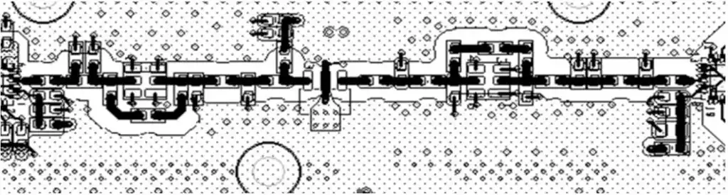
Crosstalk Mitigation
Crosstalk is unwanted electromagnetic coupling noise between PCB alignments, and it is one of the most insidious and difficult to solve problems in PCB boards. It can affect clock signals, cycles, etc.
Allowing enough space around signal alignments is the key to reducing crosstalk. Keeping all lines to and from the transceiver module as short as possible and keeping them as far away as possible from high-speed signal alignments, while minimising the distance between parallel runs, can effectively reduce crosstalk.
Other Crosstalk Mitigation Measures
Dielectric Spacing Adjustment: Reduce the dielectric spacing between the lines and their reference planes.
Introduction of coplanar structures: Use structures such as coplanar waveguides or microstrip lines.
Insertion of ground planes: Inserting ground planes between lines can reduce crosstalk by up to 50%.
Ground wrapping: Ground wrapping RF signals, interference sources, sensitive signals and other critical signals improves immunity and reduces interference to other signals.
Signal Loss Avoidance
Signal loss mainly comes from the skin effect loss and dielectric loss of the signal. The skin effect refers to the fact that at high frequencies, the current tends to flow along the surface of the conductor, resulting in a reduction of the effective conducting area and an increase in resistance, which in turn causes losses. Dielectric loss occurs when the signal passes through the dielectric material, part of the energy is converted to heat and loss.
Measures to reduce signal loss
Choose low loss materials: For very high frequency microwave circuits, it is best to use low loss laminates such as polytetrafluoroethylene (PTFE), whose dissipation factor is much lower than that of FR4. For example, ceramic-filled PTFE is the most effective solution for the tangent of the loss angle in RF PCBs.
Use conductive materials: The use of gold in RF circuits can significantly reduce losses due to the skin effect.
Optimise path length: Minimise signal transmission paths to reduce losses during signal transmission.
Impedance matching: Ensure impedance matching between components in the front-end circuit to reduce signal reflection and loss.
Reasonable Layout: Adopt reasonable layout to avoid crossing and intersecting of signal lines with interference sources and shorten the length of signal lines as much as possible.
Laminate Characteristics Considerations
Laminate characteristics are the basis of RF microwave PCB performance
When dealing with RF circuits, designers need to consider the dissipation factor and dielectric constant (Dk) values of the laminate and their variations. the dissipation factor of FR4 materials is much higher than that of high-frequency laminates such as Rogers and Nelco, which means that the use of FR4 produces high insertion losses that increase with frequency. In addition, the Dk value of FR4 can vary by up to 10 per cent, which can further change the impedance. In contrast, high-frequency boards have more stable frequency characteristics. For microwave circuits, the Dk value is related to the size of the circuit components, so designers can reduce the size of the circuit by choosing a laminate with a higher Dk value.
Despite the many advantages of RF microwave PCB, they also face challenges in practical applications. Future RF microwave PCB design will focus more on innovation in material science to develop new substrate materials with lower loss and more stable dielectric constant. With the continuous development of 5G, 6G, IoT, smart driving and other cutting-edge technologies, the performance requirements for RF microwave PCB will continues to improve, driving continuous innovation in materials, design, manufacturing and testing, and together we will build a more efficient and reliable connected world.