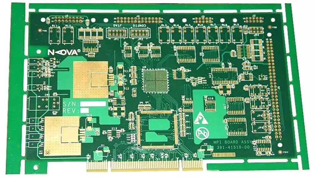
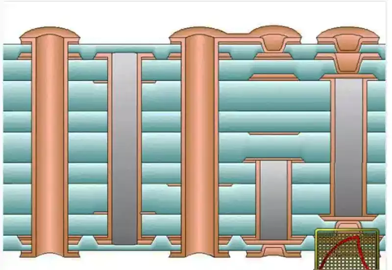
The PCB lamination process primarily involves stacking multiple layers of copper foil and dielectric materials (typically FR4, polyimide, or other composites) in a specific sequence. Under high temperature and pressure conditions, an adhesive binds these layers together tightly. The resulting multilayer PCB is a robust and fully functional circuit board capable of reliable operation within complex electronic devices.
With technological advancement and the evolution of electronic products, single-sided PCBs no longer suffice, making multilayer PCBs increasingly indispensable. Within multilayer PCB manufacturing, lamination represents a critical process warranting thorough understanding. As the name implies, lamination entails bonding individual circuit layers into a unified structure. This comprehensive process encompasses kiss pressing, full pressing, and cold pressing. During kiss pressing, resin permeates the bonding surfaces and fills voids within the circuitry. This is followed by full pressing, which bonds all remaining gaps. Cold pressing entails rapidly cooling the circuit board to stabilise its dimensions.
PCB Laminating Process Flow
Core Board Pre-treatment Stage
The primary step in PCB lamination is surface activation treatment of the inner core boards. This process involves chemical cleaning to remove surface oils and impurities, followed by mechanical roughening or chemical etching to enhance surface texture. Among these, the brownisation treatment stands as a core process. By forming a honeycomb-like oxide layer on the copper foil surface, it increases interfacial bonding strength by over 30%, effectively preventing delamination.
Prepreg Preparation Process
Prepreg specifications are precisely selected according to PCB stack-up requirements (e.g., 1080 type with 65% resin content, 7628 type with 30% resin content). High-precision PP cutting equipment is employed for trimming operations, ensuring prepreg dimensions and core board tolerances are maintained within ±0.5mm. Particular attention must be paid to the integrity of the glass fibre fabric at the cut edges, as this directly impacts the impedance performance of the conductive anode film (CAF). Any damage may lead to electromigration failure.
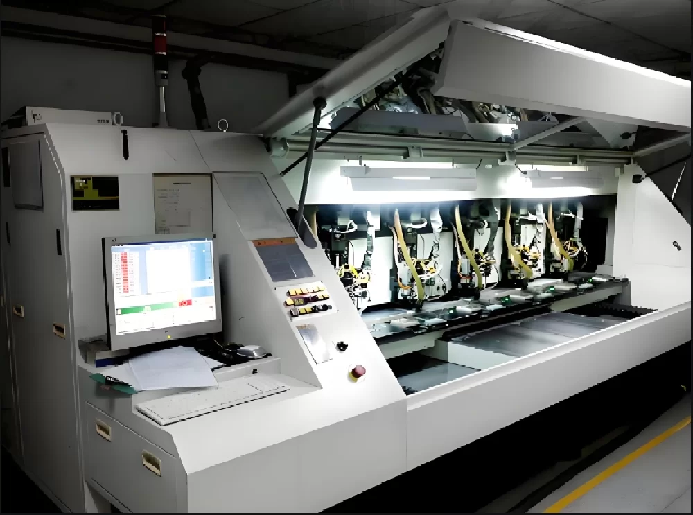
Precision Laminating Technology
When implementing multi-layer alternating stacking according to the design blueprint, a dual positioning assurance system is employed:
Mechanical Positioning: Lower-tier products commonly employ rivet positioning, using metal rivets for preliminary interlayer fixation. This method is cost-effective but offers limited precision (±0.1mm).
Optical Positioning: Higher-tier products utilise the Pin-lam system, integrated with CCD vision alignment devices, achieving ±0.02mm alignment accuracy. This is particularly suitable for precision products such as HDI boards.
Selection between positioning methods requires comprehensive consideration of product density, equipment investment, and manufacturing costs.
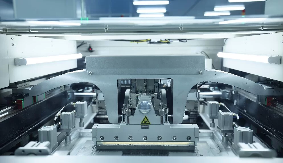
Thermal Pressing Curing Control System
After loading the laminate into the vacuum press, a three-stage temperature control curve is executed:
Preheating Stage: 80–120°C to soften resin and expel volatiles
Main Pressing Stage: 175–185°C with sustained pressure up to 35 kg/cm² for complete resin cross-linking
Pressure-holding stage: Maintain pressure at 15 kg/cm² to complete curing
The entire pressing cycle must strictly align with the material’s glass transition temperature (Tg). Overpressurisation may cause dielectric layer thickness deviations exceeding specifications, while underpressurisation may induce interlayer voids.
Stress-relief cooling process
Following hot pressing, implement a gradient cooling scheme: first reduce temperature at 5°C/min to 100°C, then allow natural cooling to ambient temperature. This process reduces residual stress by over 60%, effectively controlling panel warpage to ≤0.75%. Experimental data indicates the optimised cooling curve improves product flatness by 40%.
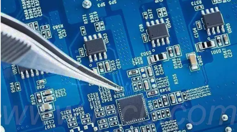
Post-Processing Finishing
The final stage comprises three core operations:
Resin Residue Removal: Utilises plasma cleaning technology to eliminate interlayer resin overflow, controlling surface roughness to Ra 0.8μm or less
CNC Forming Machining: High-precision milling machines complete contour machining with dimensional tolerances of ±0.05mm
Quality Inspection: Simultaneously performs board thickness measurement (±0.1mm accuracy), dimensional stability testing (expansion/contraction rate ≤0.05%), and X-ray interlayer inspection
Key Considerations for PCB Laminating
Temperature Control
During PCB lamination, precise temperature regulation is paramount. Excessive heat may cause material decomposition, while insufficient temperatures fail to ensure complete curing. Therefore, the heating rate, dwell time, and cooling rate must be meticulously adjusted according to the selected materials’ properties and circuit board structure to guarantee a successful lamination process.
Pressure Control
Pressure management is equally vital during PCB lamination. Insufficient pressure results in poor bonding and uneven resin flow, compromising PCB performance and reliability. For instance, uneven resin distribution may cause variations in board thickness and dielectric thickness, adversely affecting plating and impedance characteristics. Conversely, excessive pressure risks damaging inner layer traces or causing board deformation, similarly detrimental to manufacturing quality. Therefore, pressure must be appropriately regulated during lamination based on actual conditions to ensure PCB manufacturing quality and performance.
Layer Alignment Precision
Alignment deviation between layers is a critical factor during PCB lamination. Such deviation impacts proper circuit connection and smooth signal transmission. Consequently, high-precision positioning tools and processes must be employed to ensure each layer’s alignment meets specified requirements.
Material Selection
Selecting appropriate inner core boards, prepregs, and copper foil is paramount for diverse PCB applications. Material selection must holistically consider factors such as thermal resistance, moisture resistance, and electrical properties to guarantee PCB performance and quality.
Pressing Time Control
The duration of the pressing process critically impacts PCB manufacturing quality. Strict time control is essential: insufficient time prevents resin from fully curing, compromising product performance; excessive time may impair production efficiency and adversely affect material properties. Consequently, pressing time must be rigorously managed throughout PCB production to ensure the manufacture of high-quality, stable-performance PCB products.
The PCB lamination process is an interlinked sequence of steps. Only by meticulously controlling the parameters at each stage can high-quality circuit boards be produced, thereby laying a solid foundation for the stable operation of electronic products.