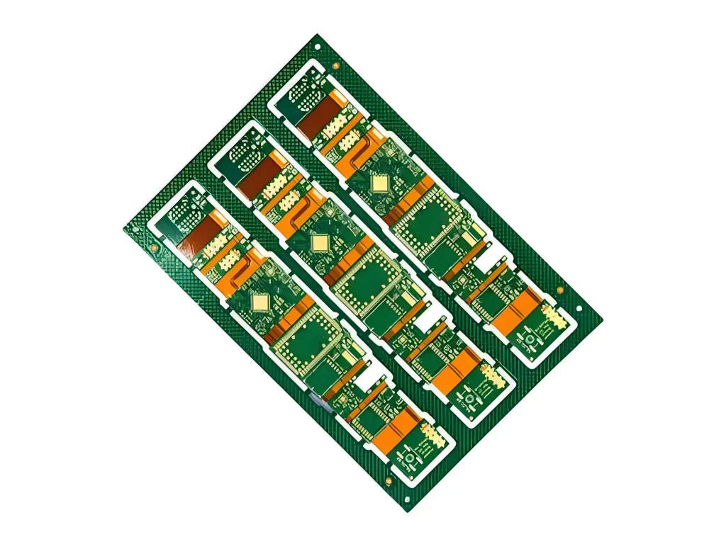
As PCBs evolve towards being lighter, thinner, smaller and more compact, rigid flex boards (also known as rigid-flex assemblies) have emerged as a key technology for reducing the size and enhancing the performance of electronic products, alongside high-density rigid boards, thanks to their three-dimensional connection and assembly capabilities.
By combining flexible circuits (FPCs) with traditional rigid boards (PCBs) through specific processes, these boards offer both flexibility and rigidity. Capable of bending and folding whilst supporting heavy components, they are widely used in products with specific requirements for internal space and reliability.
From Flexible Circuits to Rigid-Flex
Flexible circuits were initially commonly used in dynamic bending scenarios (such as the connection between a printer head and a control board); this mode of operation is referred to as ‘dynamic flex’ and typically employs a single-layer board to ensure optimal flexibility and reliability. If a flexible circuit only needs to be bent once during installation (i.e. ‘flex-to-install’) over its lifecycle, a multi-layer structure may be adopted; limited bending cycles also facilitate the production of more layers.
If components are to be mounted on a single side only, rigid material (such as FR4, without conductors) can be laminated onto specific areas of the flexible circuit to provide localised reinforcement; this design is known as a ‘rigidised flex’. It combines the advantages of both flexibility and rigidity, but is more expensive than a standard PCB.
If double-sided component mounting or ultra-thin designs are required, rigid flex boards are virtually the only option—they incorporate both rigid and flexible layers and are a type of multilayer PCB. Taking a four-layer board as an example, a typical structure features a polyimide (PI) flexible core, with copper cladding on both sides, and a single-sided FR4 rigid layer laminated on the outer layers. It is now also possible to achieve multi-layer alternating lamination of rigid and flexible layers.
Material Selection
Rigid board materials: Resin-based rigid boards are typically used, requiring strong adhesion and good heat resistance to ensure consistent expansion and contraction in the rigid-flex junction area when heated, preventing deformation.
Flexible board materials: The substrate is often selected from adhesive-free or dimensionally stable polyimide (PI), such as Kapton (thickness 12.5–75 μm). PI offers high-temperature resistance (260°C long-term, 400°C short-term), excellent electrical and mechanical properties, and is flame-retardant and chemical-resistant, making it the mainstream choice. Although polyester (PET) is inexpensive, it has poor heat resistance (melting point 250°C) and is rarely used.
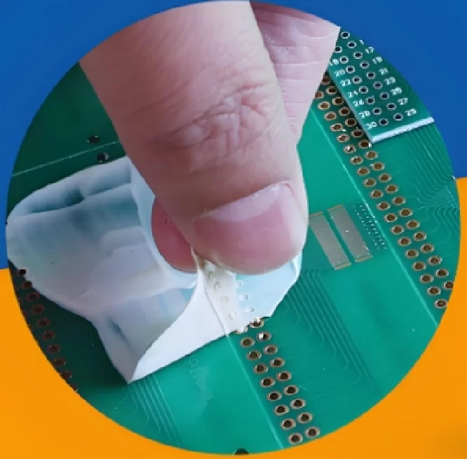
Cover film: Protects the circuit from moisture and contamination; thickness 12.7–127 μm.
Conductive layer: Rolled copper (smooth crystal structure, weak adhesion to the base film, greyish-white appearance) or electrolytic copper (coarse crystal structure, unsuitable for fine circuits, copper-red appearance). Rolled copper is recommended for fine circuits.
Reinforcement plates: Rigid materials such as FR4, PI or steel sheets are added to specific areas of the flexible board (e.g. soldering zones) to facilitate installation.
Prepreg (PP): Used for rigid-flex lamination; low-flow types (such as thin grades 106, 1080, 2116, etc.) must be selected to prevent resin overflow.
Structural Configuration
Rigid flex boards feature one or more rigid sections coexisting with flexible sections, with the circuits on the rigid and flexible layers interconnected via plated-through holes. Alternatively, multiple flexible boards can be combined with multiple rigid boards; complex electrical connections are achieved through lamination, drilling and electroplating, allowing for flexible adaptation to component mounting and debugging requirements.
Design Rules and Considerations
The design of rigid flex boards is far more complex than that of traditional PCBs; the following key rules must be observed:
1.Via Placement
Avoid placing vias in flexible areas subject to dynamic bending to prevent breakage.
Where drilling is essential, it should be kept well away from the rigid-flex interface. Generally, the distance from the via to the interface must be ≥50 mil (≥70 mil for high reliability); most manufacturers do not accept distances of <30 mil. This is the most critical design rule.
Vias on the flexible side must also comply with this distance requirement.
2.Reinforcement of Pads and Vias
Where electrically feasible, select larger pads and vias.
Ensure a smooth transition between pads and traces; avoid right angles.
Add pad tabs (support legs) to isolated pads, and incorporate teardrop-shaped extensions to via traces to enhance mechanical strength.
The larger the copper ring exposed on the solder mask, the better.
3.Routing in Flexible Areas
Avoid overlapping top-layer and bottom-layer traces along the same path, as this can lead to uneven stress distribution and damage during bending. Traces should be staggered and arranged in a criss-cross pattern.
Traces should follow curved paths (rather than 45° or 90° angles), and trace widths should not change abruptly; use teardrop-shaped curves at transitions between thick and thin sections.
Trace orientation should be as perpendicular to the bending direction as possible, and traces should be evenly distributed within the bending zone, with width maximised wherever possible.
4.Copper Laying
To improve flexibility, a mesh pattern is recommended for copper laying in the flexible zone; however, as this may affect impedance and electrical quality, a trade-off must be considered.
Solid copper may be applied more extensively in the scrap area (areas without circuits).
5.Distance between Drilled Holes and Copper (Hole-to-Copper Distance)
The standard requires a minimum distance of ≥10 mil. Due to differences in the properties of rigid and flexible materials, achieving a tighter distance is difficult to manufacture.
6.Design of the Rigid-Flex Interface
The flexible section should ideally be positioned in the middle of the laminate stack and connected to the rigid section via a prepreg.
Vias on the flexible section within the interface are equivalent to buried vias; the use of through-hole vias (PTH) should be avoided where possible.
Traces should transition smoothly, with their direction perpendicular to the bend.
7.Bending Radius
Must withstand 100,000 flex cycles without damage. The minimum bend radius R = W × T (where T is the total thickness of the flexible board; for single-sided boards W = 6, for double-sided boards W = 12, and for multilayer boards W = 24), and should not be less than 1.6 mm.
Manufacturing and Precision Considerations
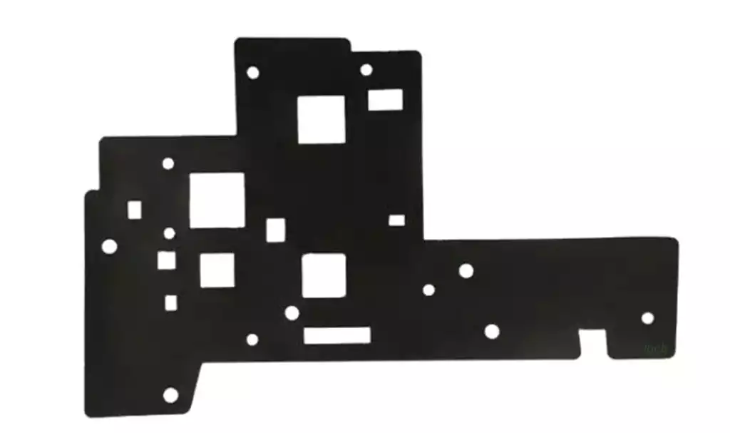
The dimensional stability of polyimide is more than three times worse than that of FR4; the flexible material will shrink significantly after copper etching. Manufacturing tolerances must be factored into the design. Furthermore, when opening windows in the rigid layers to expose the flexible areas, care must be taken to avoid removing too much rigid material, which could compromise the board’s structural integrity. Flexible board areas are typically produced using stamping, a process better suited to thin polyimide.
Common processing tolerances for flexible circuits: line width 50–75 μm, hole diameter 0.1–0.2 mm, with up to 10 or more layers. It is recommended that designers refer to the IPC-D-249 and IPC-2233 standards.
Rigid flex boards combine the advantages of rigid and flexible substrates, providing an ideal solution for high-density, three-dimensional interconnect applications. However, the diversity of materials, the complexity of the lamination process, and specific design rules (such as via clearance, curved routing, and bend radius control) present designers with entirely new challenges.