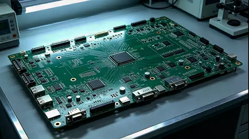
What Is a Large PCB Board?There is no single board dimension that universally defines a large PCB. Whether a circuit board is considered large depends on the manufacturing equipment, material construction, layer count, board thickness, fabrication process, and assembly requirements available for the project.
A board that is considered large on one production line may still be within the normal working range of another. This is why manufacturers may use terms such as large PCB, large-format PCB, or oversized PCB for boards that exceed their usual processing dimensions.
The physical outline is only one part of the assessment. A large PCB board also needs to be evaluated according to its layer structure, copper weight, minimum trace and spacing, hole dimensions, aspect ratio, surface finish, mechanical tolerances, and assembly requirements.
IPC maintains separate design standards for different PCB technologies and applications. For example, IPC-2221 provides generic printed board design requirements, while other standards address rigid organic boards, HDI structures, current-carrying capacity, and controlled-impedance design. The applicable requirements therefore depend on the actual construction and function of the board rather than its size alone.
Why Are Large PCB boards Used?
The main reason for using a large PCB board is usually system integration. A product may contain power circuits, processors, communication interfaces, connectors, control circuits, sensors, and other functional sections that need to occupy a relatively large physical area. Combining these functions on one board can simplify the overall mechanical architecture and reduce the number of board-to-board connections.
Large PCBs can also provide additional space for high-current copper areas, thermal structures, connectors, isolation zones, and mechanically constrained components. In industrial equipment, for example, the PCB may need to follow the dimensions of a large enclosure while still leaving room for mounting points and external interfaces.
The decision to use a large board should therefore be based on the complete product architecture. Increasing the board size simply to avoid circuit partitioning may introduce manufacturing and assembly problems if the larger format is not considered during the initial design.
Why Does a Large PCB Become More Difficult to Manufacture?
The manufacturing challenges of a large PCB board are closely related to scale. When the physical dimensions increase, small variations that would have little practical impact on a smaller board can become more significant across the entire board.
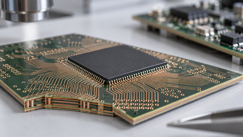
This is particularly important for mechanical stability. During PCB fabrication, laminate, copper and resin systems are exposed to heat, pressure and dimensional changes. If the construction is not mechanically balanced, the resulting stresses can contribute to bow or twist. The effect can become more noticeable as the board becomes larger.
Recent manufacturing guidance for large-format PCBs also identifies warpage, layer registration, copper distribution, solder mask alignment and handling as important considerations when the board exceeds a manufacturer’s normal processing range.
This is why a large PCB should be treated as a complete manufacturing structure rather than simply a larger drawing.
Large PCB Warpage Requires Attention From the Design Stage
Warpage is one of the most important issues to consider when designing a large PCB.
A multilayer board contains different materials and copper patterns that respond differently during lamination and subsequent thermal processes. When the copper distribution or stack-up is significantly unbalanced, the stresses within the board can become uneven.
For a small board, the resulting deformation may remain manageable. On a large board, however, the same imbalance can affect a much greater physical area and may interfere with assembly, mechanical installation, or the alignment of connectors and mounting features.
Copper distribution should therefore be reviewed across the entire board rather than only around individual circuit sections. The stack-up should also be designed with mechanical symmetry in mind wherever the electrical requirements allow it.
IPC specifically identifies DFM as an important part of the product development process and provides DFM profiles based on its design and performance standards.
For large boards, this means DFM should happen while the stack-up, copper distribution, board outline and mechanical features can still be changed. Waiting until fabrication to discover that the board is difficult to manufacture leaves far fewer options for correction.
Copper Distribution Matters on a Large PCB
Copper serves an electrical purpose, but its distribution also affects the physical behavior of the PCB.
A board may contain large power planes in one area, dense copper around high-current circuits, and relatively open routing regions elsewhere. If similar differences occur between opposing layers, the finished board can have an uneven mechanical structure.
This does not mean that every PCB must have exactly the same copper percentage on every layer. Functional requirements still take priority. Instead, the objective is to identify major differences in copper distribution and determine whether the stack-up and manufacturing process can accommodate them.
Recent technical discussions of PCB warpage continue to emphasize copper balance and stack-up symmetry as important design considerations, particularly for multilayer boards.
For a large PCB board, the review should be performed across the complete board. A copper pattern that looks reasonable in one corner may still create an imbalance when considered together with the rest of the layer.
Mechanical Design Becomes More Important as Board Size Increases
Large PCB design is closely connected to the mechanical design of the product.
Mounting holes, connectors, cutouts, board edges and enclosure interfaces should be established before routing is finalized. The larger the board, the more important it becomes to define which features control the mechanical position of the PCB.
For example, a connector located near one end of a long board may need to align with a corresponding interface on the enclosure. A dimensional error that seems small at the CAD level can become a practical problem when several mounting and interface points are distributed across a large distance.
For this reason, critical mechanical dimensions should have clearly defined references, and the manufacturing drawing should distinguish between general dimensions and dimensions that directly affect system assembly.
Large PCB Board Manufacturing Also Requires Suitable Fabrication Equipment
A board may satisfy the electrical requirements of the design and still be unsuitable for a particular manufacturing line.
The actual production capability depends on more than the nominal working area of a machine. Drilling, imaging, lamination, plating, etching, solder mask, surface finishing, inspection and handling all need to accommodate the finished board.
This is particularly relevant when the board approaches or exceeds the dimensions normally processed by a factory. Current large-format PCB manufacturing guidance shows that manufacturers may have different maximum dimensions depending on layer count and construction, which is another reason a fixed industry-wide definition of “large PCB” is not appropriate.
The practical question is therefore not simply whether the board fits on one machine. The complete fabrication route must be evaluated.
Large PCB Assembly Is a Separate Manufacturing Consideration
A large bare PCB may be manufacturable while the assembled board creates additional challenges.
During SMT assembly, the board passes through several processes, including solder paste printing, component placement, reflow soldering and inspection. Each process needs to accommodate the board’s dimensions, thickness, weight and mechanical behavior.
For example, the stencil printer needs to support the complete board during paste deposition. The conveyor must transport the board without excessive movement or sagging. During reflow, the board needs adequate support so that its deformation remains within the acceptable process range. Inspection equipment must also accommodate the finished assembly.
Recent large-format assembly guidance makes the same point: the maximum size supported by an individual placement machine does not necessarily represent the maximum size that can pass through the complete SMT line. The printer, conveyor, reflow oven, AOI, testing equipment and other operations all need to be considered together.
This distinction is particularly important when a project moves from PCB fabrication to PCBA production.
How Should a Large PCB Be Designed for Manufacturing?
The best time to address large PCB manufacturing problems is before the design is released.
The board outline should be reviewed together with the manufacturing process, while the stack-up should be evaluated for both electrical and mechanical balance. Copper distribution should be checked across all relevant layers, especially where large power planes or substantial differences in copper density exist.
The design should also provide enough manufacturing margin around holes, traces, spacing, board edges and mechanical features. These values should be based on the selected manufacturing process rather than copied from a generic PCB design rule.
IPC’s DFM guidance demonstrates why manufacturing rules should be connected to the actual PCB design and the applicable performance requirements. Its DFM profiles cover different combinations of performance classes and producibility levels and are based on multiple IPC standards.
For a large PCB, this engineering review can help identify problems with board dimensions, registration, copper balance, drilling, mechanical interfaces and assembly support before the project reaches production.
What Should Be Checked Before Manufacturing a Large PCB?
Before production begins, the board should be reviewed as both an electrical design and a physical manufacturing structure.
The finished dimensions should be compared with the actual fabrication capability. The stack-up should be checked for symmetry and material compatibility, while copper distribution should be reviewed across the complete board instead of layer by layer in isolation.
Mechanical features deserve a separate review because mounting holes, connectors and cutouts often determine whether the finished PCB can be installed correctly. Drilling and registration requirements should also be checked against the selected fabrication process.
If the PCB will be assembled, the review needs to continue into the SMT process. Board support, stencil printing, component placement, reflow, inspection and electrical testing should all be considered before the production package is released.
This approach is more reliable than asking for a single maximum board size because the same physical dimensions can create very different manufacturing requirements depending on thickness, layer count, copper weight and assembly configuration.
What Information Is Needed for a Large PCB Project?
When requesting a large PCB quotation or manufacturing feasibility review, providing only the board length and width is usually insufficient.
The manufacturing package should define the board outline, layer count, finished thickness, copper weight, material requirements, surface finish, hole requirements and important dimensional tolerances. If the design includes controlled impedance, special thermal requirements or other critical characteristics, those requirements should also be clearly documented.
For PCB assembly, the manufacturing package normally needs additional information related to components and assembly. A bill of materials, component placement data, assembly drawings and testing requirements can help the manufacturing team evaluate the complete process rather than only the bare board.
IPC also promotes standardized manufacturing data formats such as IPC-2581 for transferring information required for PCB fabrication, assembly and inspection.
Complete documentation becomes particularly valuable for large PCB projects because more manufacturing variables can affect the final result.
Large PCB Board vs. Standard PCB
The difference between a large PCB and a standard PCB is not simply the number shown on a ruler.
A conventional PCB may fit comfortably within the normal working range of a fabrication and assembly line. A large PCB can place additional demands on mechanical stability, material behavior, handling, equipment compatibility and process control.
This does not mean that every large board is inherently difficult to manufacture. A properly engineered large PCB can be produced reliably when its electrical design, mechanical construction and manufacturing process are considered together.
The important difference is that the margin for overlooking mechanical and process limitations becomes smaller as the physical size increases.
A large pcb board is more than a standard circuit board with a larger outline. Its size can influence mechanical stability, copper distribution, dimensional control, fabrication accuracy, handling and the way the finished board moves through an SMT assembly line.
For this reason, large PCB board projects should be evaluated from the design stage. A suitable stack-up, balanced copper distribution, well-defined mechanical references and realistic manufacturing tolerances can make the board easier to fabricate and assemble. At the same time, the complete production route should be reviewed rather than judging feasibility from the capacity of a single machine.