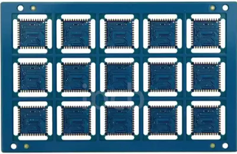
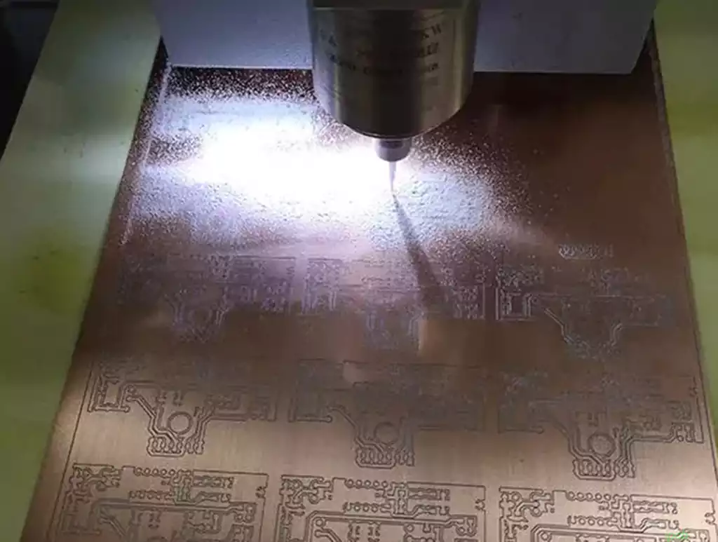
Laser engraving pcb board is a kind of efficient and precise printed circuit board processing equipment, which adopts the laser technology, can carry out high-precision engraving, laser engraving, etc. on the surface of PCB, so as to realize the marking, marking, layout, cutting and other processing of the circuit board, which provides important technical support for the production of circuit boards.
Laser marking is the use of high energy density laser on the PCB substrate for local irradiation, so that the surface material vaporization or discoloration, thus leaving a lasting mark. This kind of non-contact processing, can be in a very small amplitude marking out very clear two-dimensional code, to ensure high precision at the same time to ensure high quality. At the same time, the laser marking will not wear out due to high and low temperatures, changes in acidity and alkalinity, and external friction, and does not require the assistance of chemicals, so there is no negative effect on personnel safety and the environment.
In the pcb board laser marking lettering application, the use of more UV laser marking and CO2 laser marking. UV laser marking and CO2 laser marking have become the technology of choice for surface marking of PCB boards due to their low thermal impact, good processing results, high precision and speed.
A large number of printed circuit boards can also be operated using fully automated laser marking machine, only need to install automated flow part on the UV laser marking machine and CO2 laser marking machine to realize the automatic loading and unloading of PCB boards, to facilitate the circuit boards directly for marking and processing, without the need to transport to the marking and processing of the unified processing of the place, to improve the marking efficiency, to improve the processing of the coherence of a circuit board laser marking machine. Greatly improve the efficiency and cost savings.
Advantages
- good quality, wear resistance, circuit board surface marking clear and beautiful, can be labeled with a variety of LOGO, pattern, two dimensional code, text, and the pattern is engraved directly on the material above, wear resistance is more prominent;
- High processing precision. Laser beam emitted by the laser is focused after the minimum spot diameter can reach 10um (UV laser), in dealing with complex graphics and precision processing with a small big help;
- High efficiency, simple operation and cost reduction. Users only need to set up the parameters on the computer can directly marking, in just a few seconds to a dozen seconds to complete the material surface marking.
- Non-destructive marking. Laser marking using non-contact processing, the laser head does not need to contact the surface of the material, so do not need to consider the damage to the material;
- Wide range of use, safety and environmental protection. All kinds of thin metal/non-metal materials can be marked;
- Stable performance, long service life of the equipment. With the development of technology, the service life of the laser is greatly increased, and the service life of the equipment is greatly lengthened.
Scope of application
PCB laser marking machine is commonly used in electronic manufacturing industry, mainly used for circuit board marking, logo, layout and cutting and other dispositions. Application scope includes:
- Electronic manufacturing industry: can be applied to electronic parts, pcb plate, LED light bar, display screen and other electronic products consumption processing.
- Automobile manufacturing industry: can be applied to automobile parts, instrument panels, instrumentation and other automotive products consumption and processing.
- Medical equipment manufacturing industry: can be applied to medical equipment, surgical instruments, medical equipment and other medical products consumption and processing.
- Jewelry manufacturing industry: can be applied to jewelry, diamonds and other valuables engraving, engraving and other disposal.
Laser engraving pcb board with its high efficiency, precision features, is gradually changing the traditional way of printed circuit board processing, leading the circuit board processing industry a new chapter. For the sustainable development of the electronics manufacturing industry provides strong technical support. In the future, with the continuous progress of technology and application areas continue to broaden, it will play a more important role in the field of circuit board processing, to promote the sustainable development of electronic manufacturing and innovation.